Printed circuit board routing and power delivery for high frequency integrated circuits

Inactive Publication Date: 2005-05-31
INTEL CORP
View PDF22 Cites 63 Cited by
  • Summary
  • Abstract
  • Description
  • Claims
  • Application Information

AI Technical Summary

Problems solved by technology

Such large inductances for signals of the top signal layer 8 may present challenges for a PCB design to be us

Method used


Image

  • Printed circuit board routing and power delivery for high frequency integrated circuits
  • Printed circuit board routing and power delivery for high frequency integrated circuits
  • Printed circuit board routing and power delivery for high frequency integrated circuits

Examples


Embodiment Construction

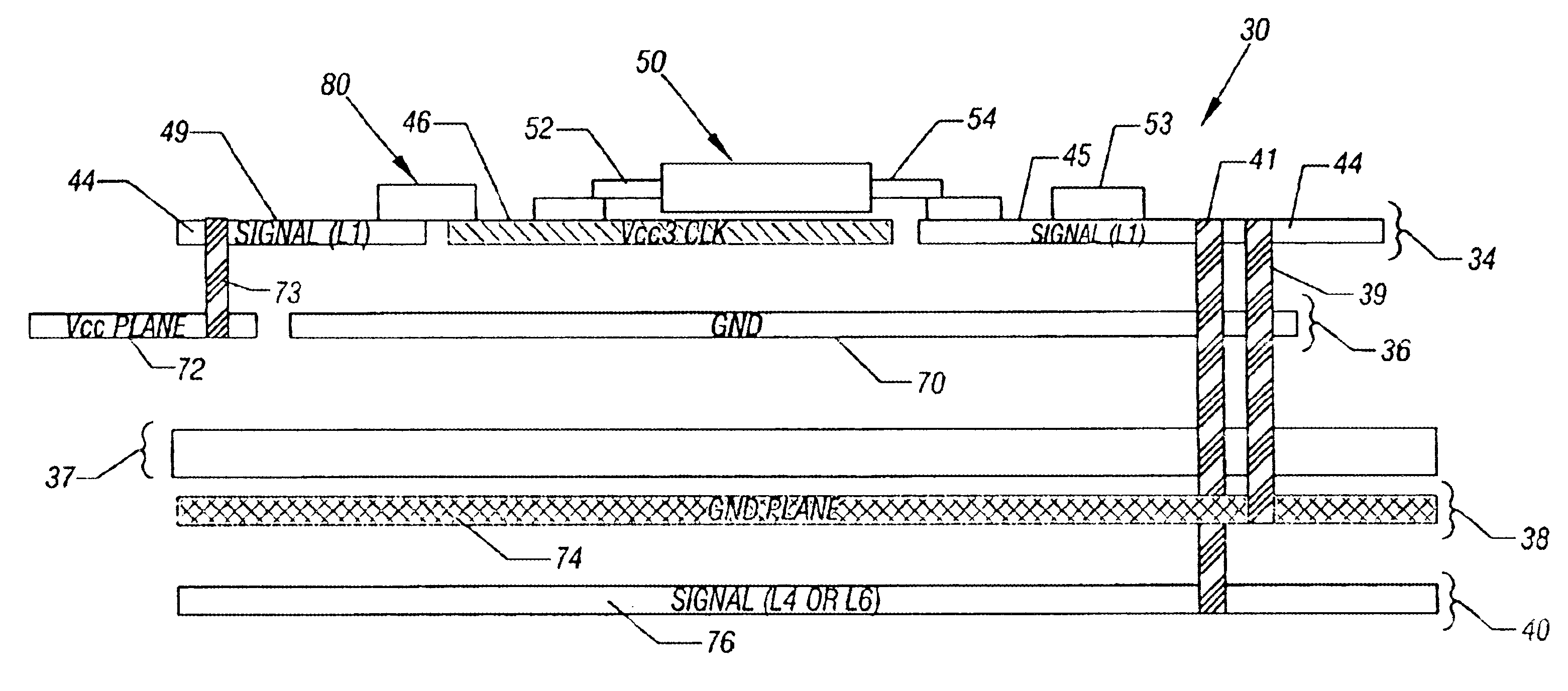
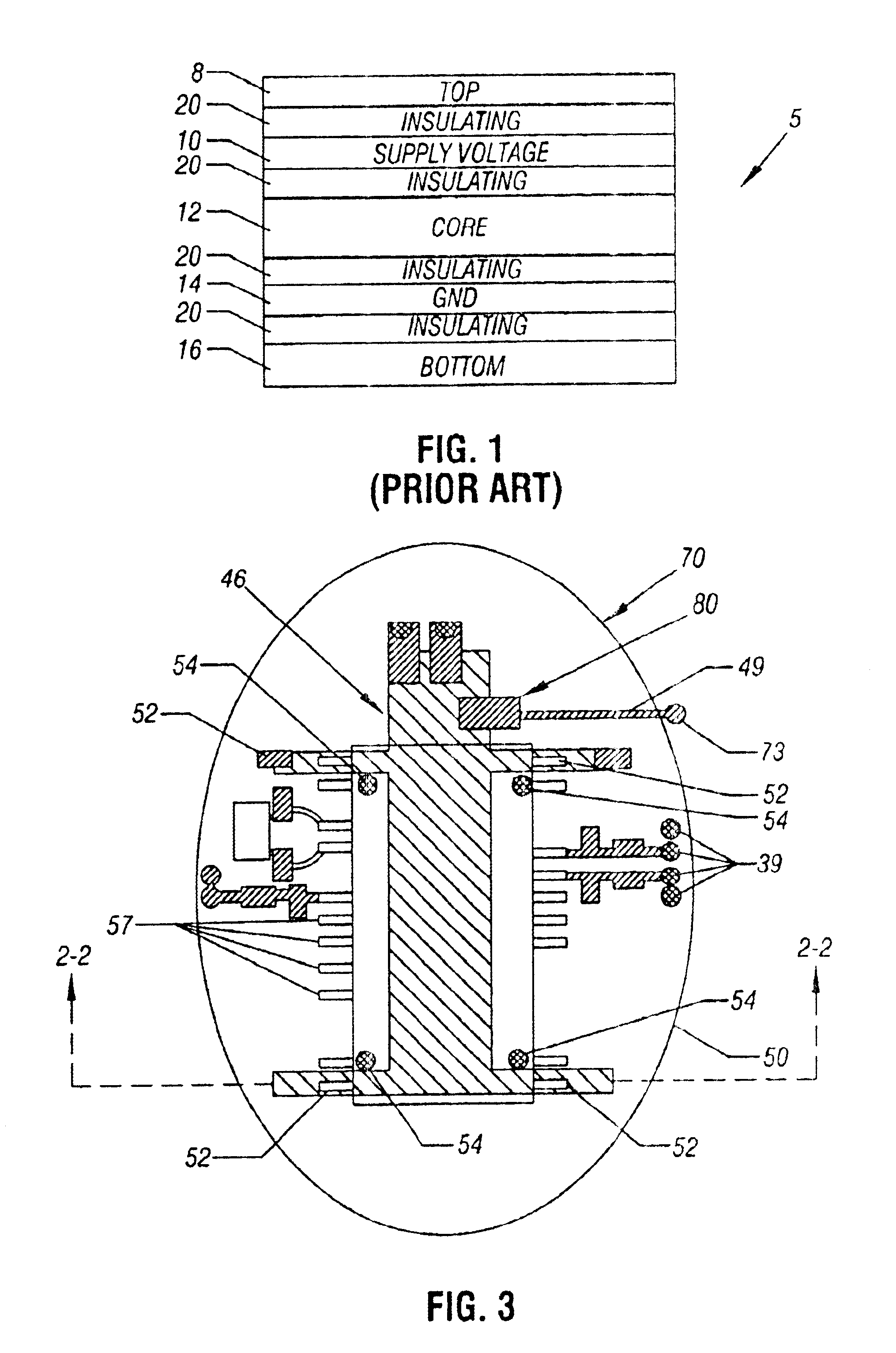
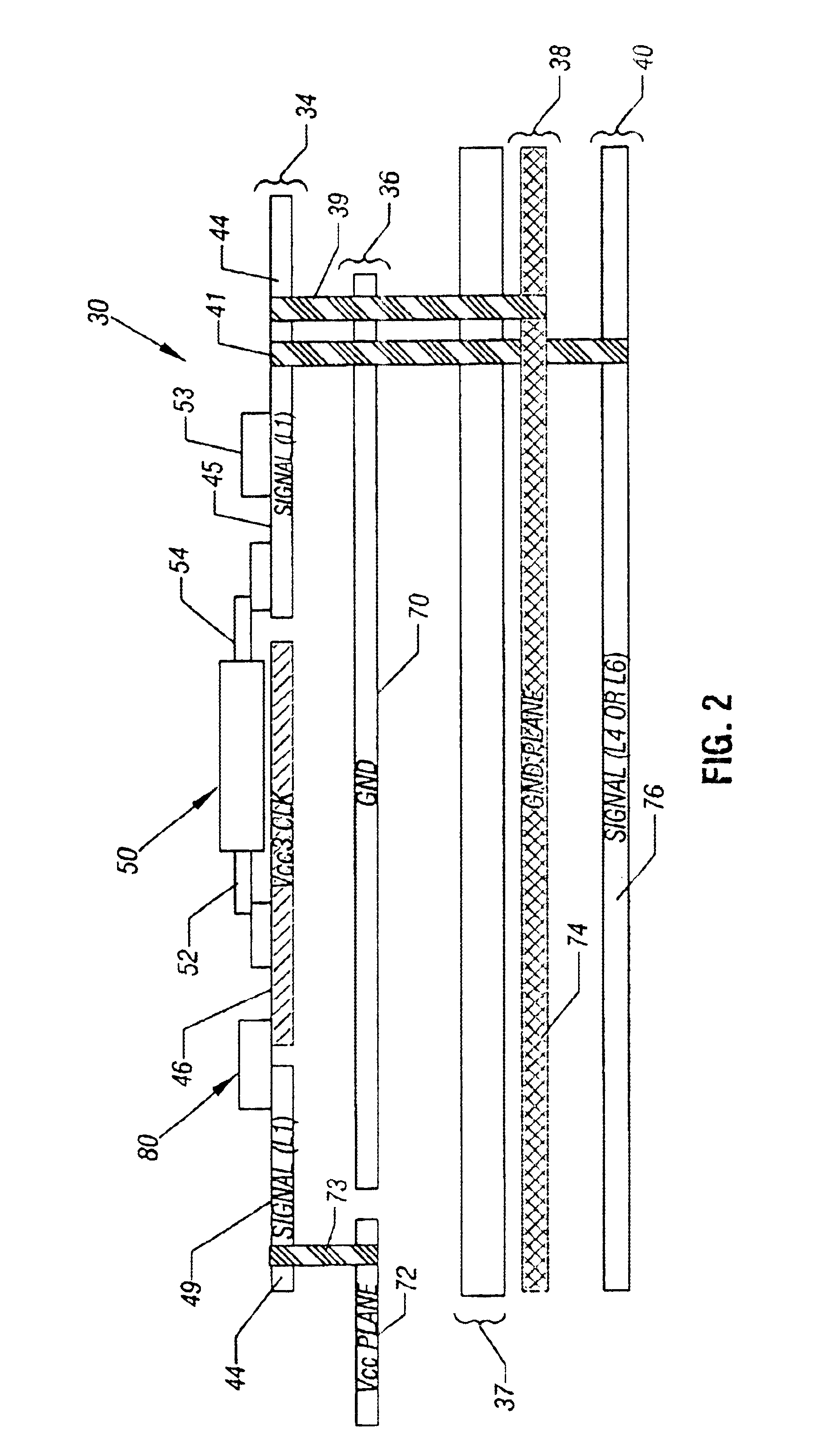
[0012]Referring to FIG. 2, an embodiment 30 of a printed circuit board (PCB) 30 in accordance with the invention is constructed to minimize the degree of noise that the PCB 30 induces on high frequency signals that propagate across the PCB 30. In particular, the PCB 30 includes a top signal layer 34 that includes embedded supply voltage planes 46 (one embedded supply voltage plane 46 being depicted in FIG. 2) and an adjacent supply voltage plane layer 36 that is located below the layer 34 and includes embedded ground planes 70 (one embedded ground plane 70 being depicted in FIG. 2). As described below, each high frequency component that is mounted on the top side of the PCB 30 is located near and is coupled to one embedded supply voltage plane 46 and one embedded ground plane 70 for purposes of minimizing inductances that may otherwise be introduced by the PCB 30. Although a four layer PCB is described, the arrangements described herein are not limited to four layer PCBs and thus, m...


PUM


Abstract

A printed circuit board includes a signal layer and a supply voltage plane layer. The signal layer includes traces to communicate signals that are not associated with regulated supply voltages. The supply voltage plane is embedded in the signal layer to supply power to multiple supply voltage pins of a component that is mounted to the printed circuit board. The printed circuit board may also include a supply voltage plane layer to communicate a supply voltage. A ground plane may be embedded in the supply voltage plane layer to provide ground connections to multiple pins of the component.

Description

BACKGROUND[0001]The invention generally relates to printed circuit board routing and power delivery for high frequency integrated circuits.[0002]Referring to FIG. 1, a typical printed circuit board (PCB) 5 includes various conductive layers and a substrate, or core 12, that supports circuit components (mounted to the PCB 5) and the conductive layers of the PCB 5. As an example, in a four layer PCB configuration, two of the four layers may be located one side (called a “top side” for purposes of simplifying the discussion) of the core 12, and two layers may be located on the opposite, bottom side of the core 12.[0003]As a more specific example, the PCB 5 depicted in FIG. 1 has four conductive layers, or is a “four layer PCB,” that includes such layers as a top signal layer 8, a layer that includes etched out conductive traces to route various communication signals that are associated with components that are mounted to the PCB 5 above the layer 8. The PCB 5 also includes a supply vol...

Claims


Application Information

Patent Timeline
IPC IPC(8): H05K1/02H05K3/46
CPCH05K1/0233H05K1/0237H05K1/0243H05K2201/10689H05K2201/086H05K2201/09336H05K2201/09345H05K3/4644
Inventor KELLY, CHRISTOPHER J.KRIEGER, JEFFREY L.ASKEW, RAYMOND P.
Owner INTEL CORP
Why Eureka
Try Eureka