Selective heating using flash anneal

a technology of flash anneal and selective heating, which is applied in the direction of semiconductor devices, basic electric elements, electrical equipment, etc., can solve the problems of structure breaking, shattering or becoming otherwise unusable, and processing times already approaching unreasonable durations, so as to achieve faster production rate, less breakage, and higher volume production

Inactive Publication Date: 2005-06-28
WAFERMASTERS
View PDF5 Cites 29 Cited by
  • Summary
  • Abstract
  • Description
  • Claims
  • Application Information

AI Technical Summary

Benefits of technology

[0016]The present invention provides a method for producing SOI wafers, including SOQ and SOF wafers. The wafers can be made with less breakage and at a faster production rate so that higher volume production can be achieved.
[0019]Typical, heat treatments of SOI wafers have required heating of the entire bulk SOI wafer. The selective heating of primarily just the region defined by the implanted hydrogen ions of the silicon substrate allows for causing the agglomeration of the hydrogen implantation without creating stresses due to inconsistent thermal expansion coefficients of the substrate materials, thus avoiding causing the destruction of the SOI wafer. Since the flash anneal process is substantially instantaneous, the production time is increased as well.

Problems solved by technology

Unfortunately, the force of deformation caused by the difference in the thermal expansion coefficient of support substrate 102 and SiO2 layer 104 can subject the SOI structure to stresses which cause the structure to break, shatter or become otherwise unusable.
Increasing the time for conducting heat treatments may help to reduce the stress effects, however, processing times are already approaching unreasonable durations.

Method used


Image

  • Selective heating using flash anneal
  • Selective heating using flash anneal
  • Selective heating using flash anneal

Examples


Embodiment Construction

[0035]As used herein, the word “flash” includes it ordinary meaning as generally understood by those of ordinary skill in the art. This definition includes the definition that flash means to give off light energy suddenly or substantially instantaneous (or in transient bursts) for a duration of time between about 1 nanosecond and about 10 seconds.

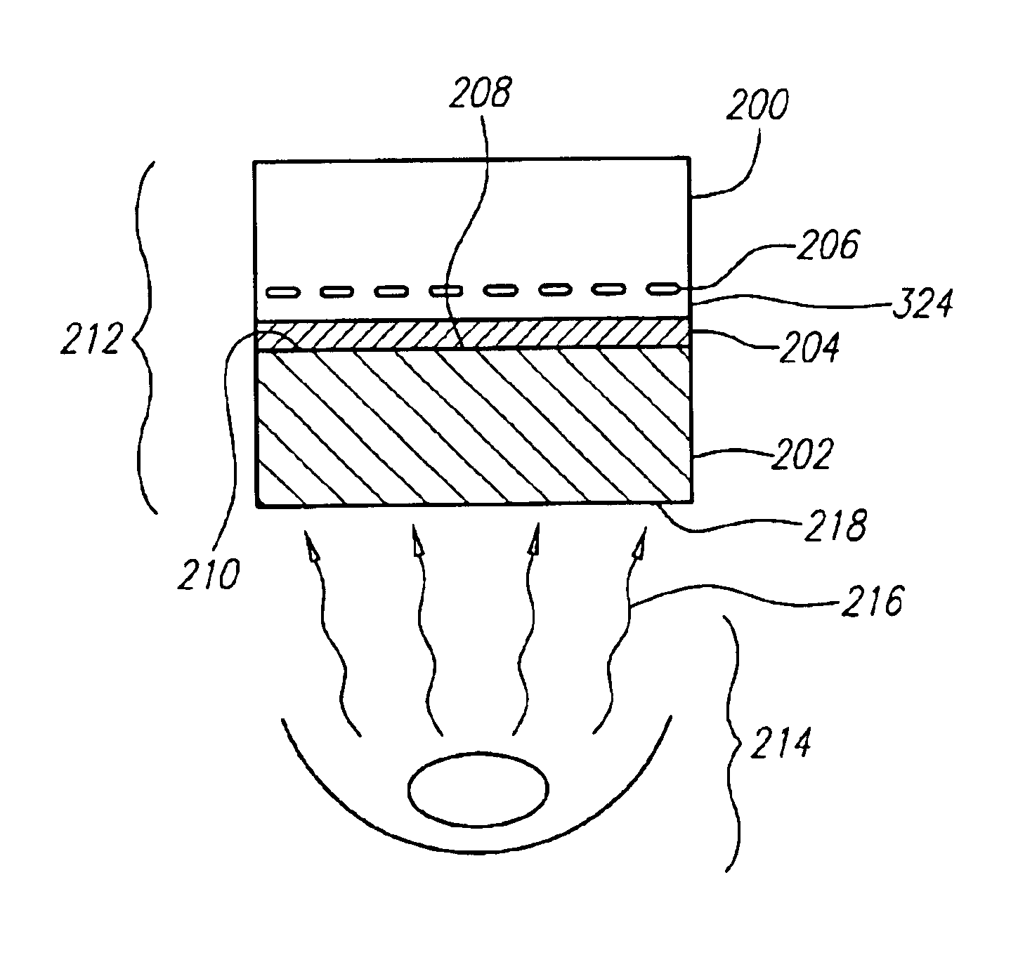
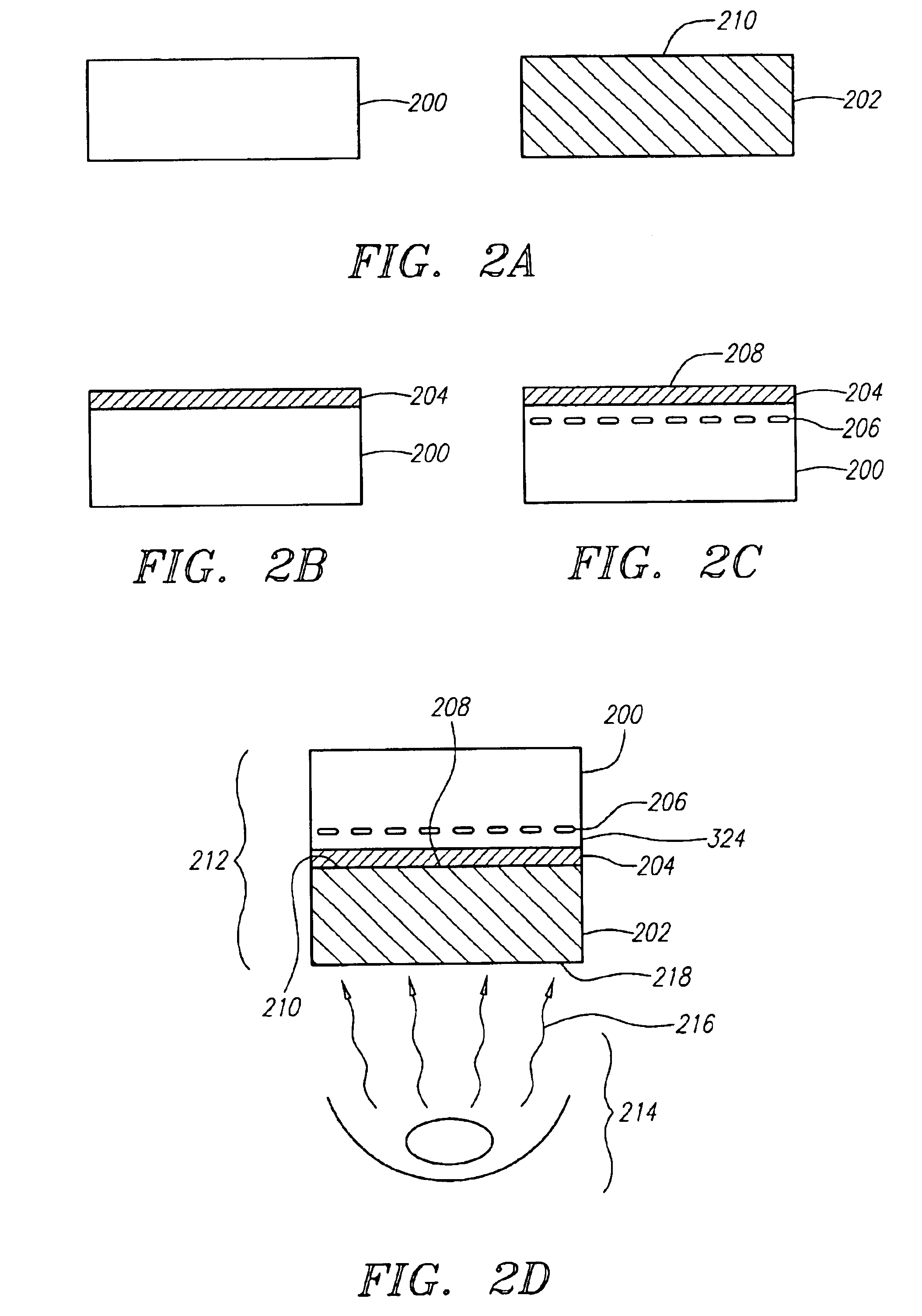
[0036]The active layer of a portion of a semiconductor wafer is well known in the semiconductor manufacturing industry as that portion of the wafer in which semiconductor devices are formed, such as transistors, diodes, resistors, and capacitors. For example, referring to FIG. 3, active layer 302 extends from surface 304 of a wafer down to a depth α below surface 304. In this example, with no intent to be limiting, the depth α is typically between about 0.05 μm and 1 mm, but will vary with the process and device feature size.

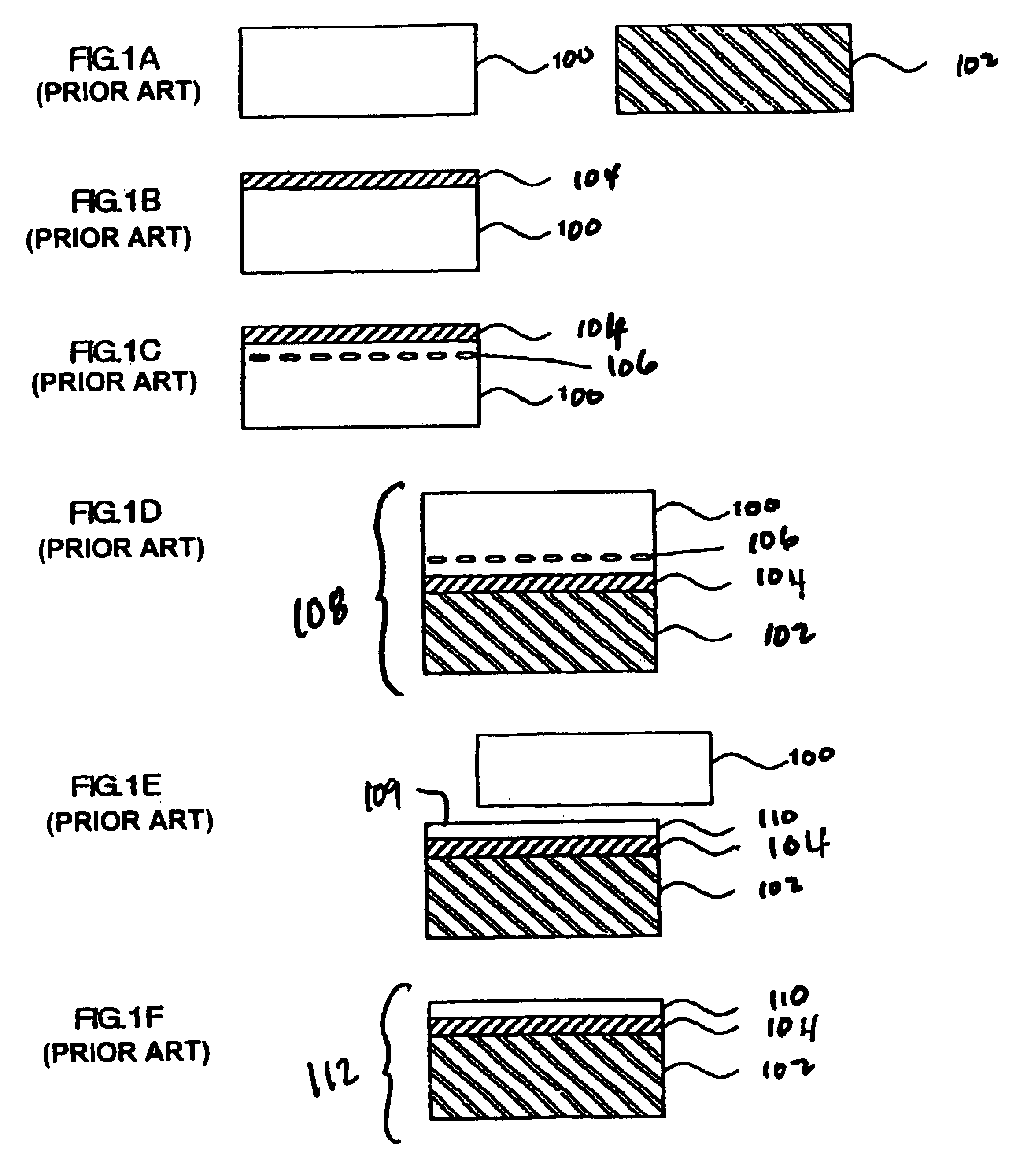
[0037]FIGS. 2A to 2D are simplified cross-sectional views illustrating respective steps of a method of fabricating a ...


PUM

PropertyMeasurementUnit
depthaaaaaaaaaa
depthaaaaaaaaaa
temperatureaaaaaaaaaa

Abstract

A process, which includes implanting hydrogen ions into a silicon substrate, overlaying the silicon substrate on to a support substrate, and applying a flash anneal heat treatment to the silicon and support substrates to cause the silicon substrates to separate at a region defined by the implanted hydrogen ions.

Description

BACKGROUND OF THE INVENTION[0001]1. Field of the Invention[0002]This invention generally relates to semiconductor manufacturing equipment and, more particularly, to a method of manufacturing a semiconductor device with a SOI structure.[0003]2. Related Art[0004]A silicon-on-insulator (“SOI”) structure includes an active silicon layer on an electrically insulating silicon oxide layer. The creation of SOI wafers represents an intermediate step between the fabrication of the polished, bulk wafers and the creation of electronic components.[0005]Semiconductor manufacturers can fabricate integrated circuits (ICs or chips) on the top layer of the SOI wafers using the same processes used on plain silicon wafers. The embedded layer of insulation enables the SOI-based chips to function at significantly higher speeds while reducing electrical losses. The result is an increase in performance and a reduction in power consumption.[0006]Many methods have been provided related to the formation of an...

Claims


Application Information

Patent Timeline
Patent Type & Authority Patents(United States)
IPC IPC(8): H01L21/00H01L21/324H01L21/762
CPCH01L21/67115H01L21/76838H01L21/76254H01L21/324Y10S438/967Y10S438/918
Inventor YOO, WOO SIK
Owner WAFERMASTERS
Why Eureka
Try Eureka