

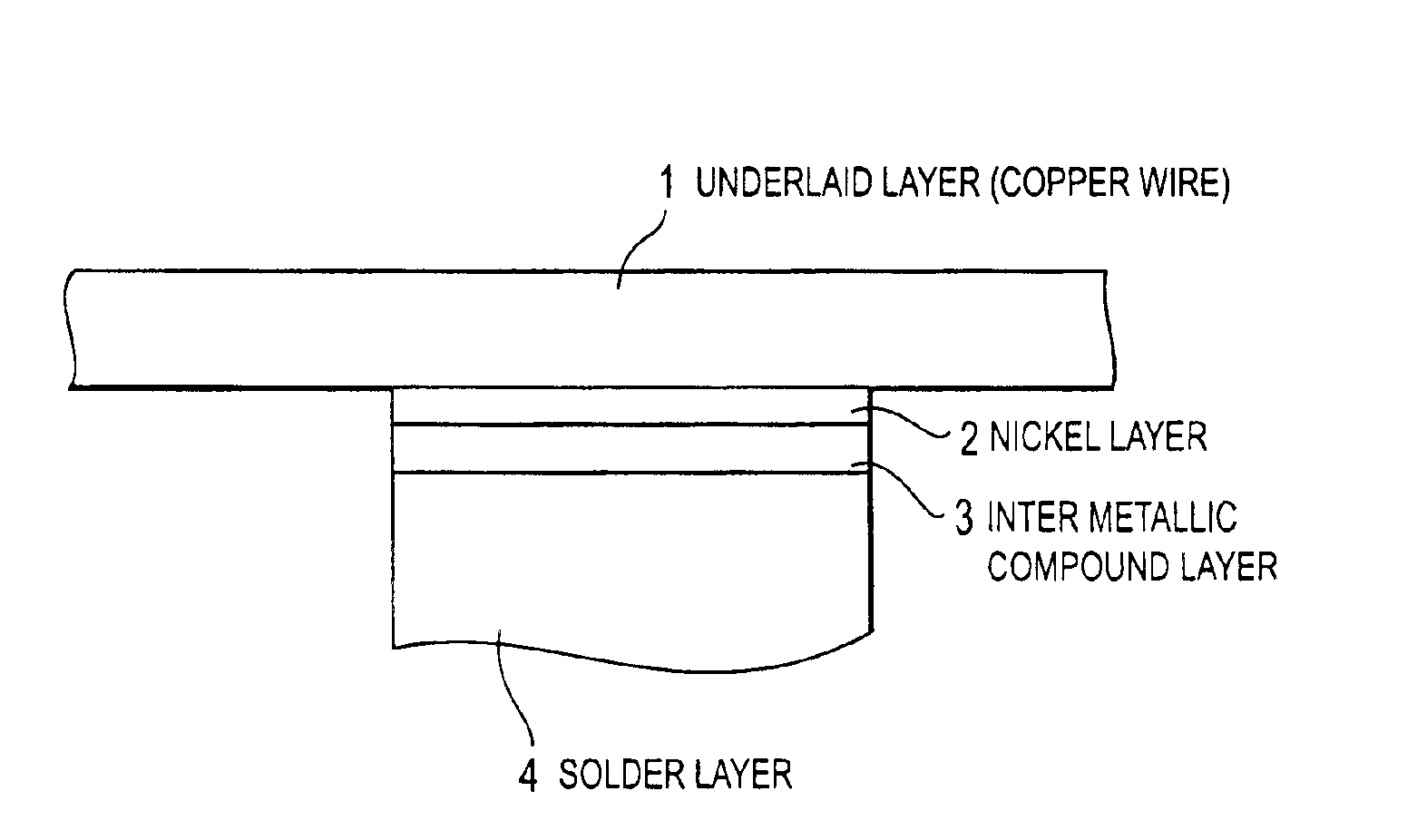
High-strength solder joint
a solder joint, high-strength technology, applied in the direction of heat measurement, instruments, semiconductor/solid-state device details, etc., can solve the problems of low strength of the solder joint, small electrode area of the soldering, and inability to meet the requirements of the soldering process
- Summary
- Abstract
- Description
- Claims
- Application Information
AI Technical Summary
Benefits of technology
Problems solved by technology
Method used
Image

Examples
examples
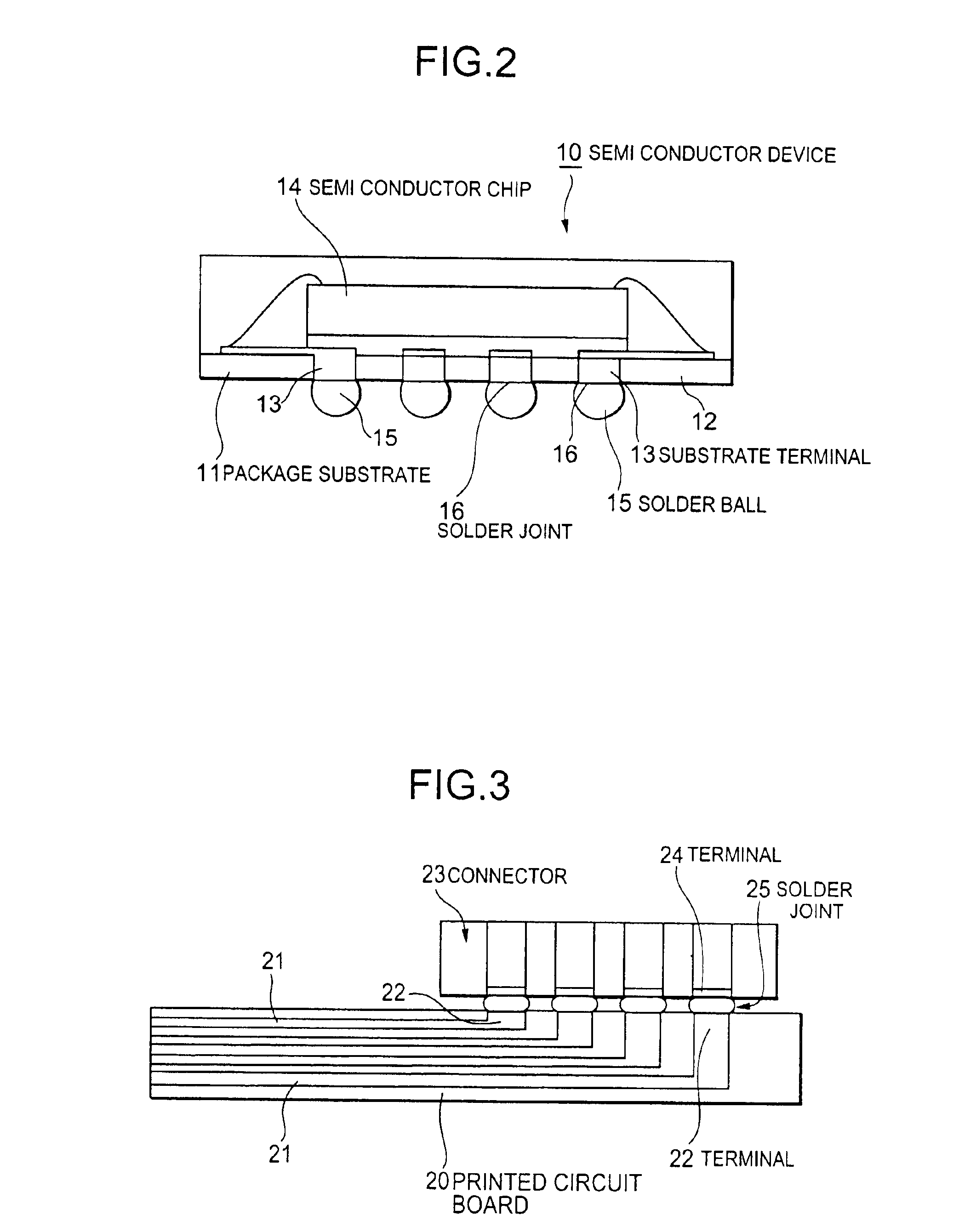
[0062]To confirm that the embodiment provides a high-strength solder joint, a destructive lifetime inspection of samples A, B, C, and D was made under conditions as shown in the following table, taking as an example a printed circuit substrate as shown in FIG. 8.
[0063]
TABLESAMPLESAMPLESAMPLE ASAMPLE BCDDEVICEBGALGABGALGATYPESOLDERSn—Ag—CuSn—PbBALLeutecticSOLDERSn—Ag—CuSn—Ag—CuSn—PbSn—PbPASTEeutecticeutecticREFLOW235235235235PEAK TEMP.(DEGREESCENTI-GRADE)
1. Substrates to be Inspected
[0064]A substrate to be inspected is formed by soldering electronic parts to a printed circuit substrate (100×40 mm). Here, as shown in the above table, four substrates having different compositions of solder and different types of mounted device (samples A, B, C, and D) are prepared. The details of solder and the printed circuit substrate are described hereafter.
1.1 Solder
[0065]The samples A and B use an Sn-3.5Ag-0.75Cu % by weight solder. The samples C and D use an Sn—Pb eutectic solder in a comparative...
PUM
| Property | Measurement | Unit |
|---|---|---|
| diameter | aaaaa | aaaaa |
| diameter | aaaaa | aaaaa |
| diameter | aaaaa | aaaaa |
Abstract
Description
Claims
Application Information