Differential column readout scheme for CMOS APS pixels

a pixel and column readout technology, applied in the field of semiconductor imaging devices, can solve the problems of uncorrelated noise components, affecting the image quality of the image sensor, so as to improve the consistency of pixel to pixel output, improve the dynamic range of pixel output, and improve the effect of substrate and other common mode nois

Inactive Publication Date: 2005-07-19
APTINA IMAGING CORP
View PDF7 Cites 48 Cited by
  • Summary
  • Abstract
  • Description
  • Claims
  • Application Information

AI Technical Summary

Benefits of technology

[0018]The present invention provides an improved column readout circuitry and method of operation which minimizes substrate and other common mode noise during a read out operation. The circuit improves the consistency of the pixel to pixel output of the pixel array and increases the dynamic range of the pixel output. This is accomplished by obtaining a differential readout of the reset signal and image signal from a desired pixel along with the reset signal and charge sig...

Problems solved by technology

This increases substrate noise coupling to a pixel, which can compromise the signal to noise ratio of the image sensor core.
The substrate noise occurs when spurious noise signals are injected locally into the substr...

Method used


Image

  • Differential column readout scheme for CMOS APS pixels
  • Differential column readout scheme for CMOS APS pixels
  • Differential column readout scheme for CMOS APS pixels

Examples


Embodiment Construction

[0044]In the following detailed description, reference is made to the accompanying drawings, which form a part hereof, and in which is shown by way of illustration specific embodiments in which the invention may be practiced. These embodiments are described in sufficient detail to enable those of ordinary skill in the art to make and use the invention, and it is to be understood that structural, logical or other changes may be made to the specific embodiments disclosed without departing from the spirit and scope of the present invention.

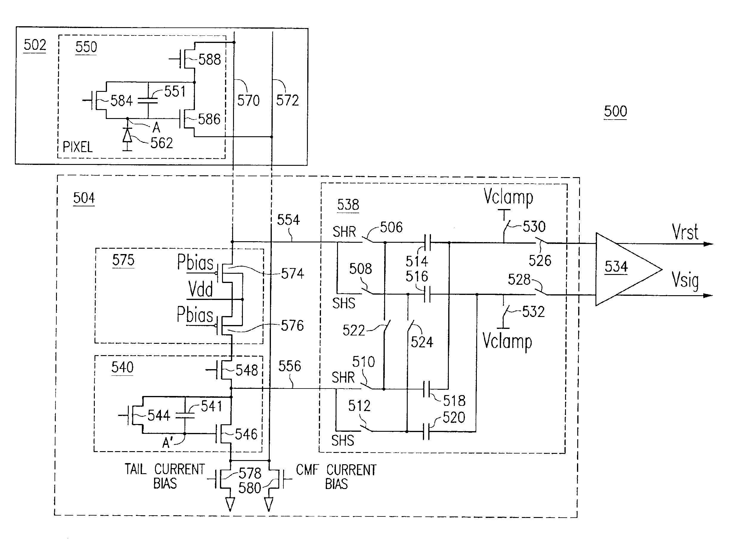
[0045]To minimize additional new noise, the present invention utilizes a differential column readout circuit using two signal sources—a desired pixel and a reference circuit—as the sources of reference differential signals which are combined and output from the column readout circuit 504. In an exemplary embodiment, shown in FIG. 5, there is no actual photosignal from the reference circuit 540 available; however a comparison value from the reference ...


PUM


Abstract

The present invention provides an improved column readout circuitry and method of operation which minimizes substrate and other common mode noise during a read out operation. The circuit improves the consistency of the pixel to pixel output of the pixel array and increases the dynamic range of the pixel output. This is accomplished by obtaining a differential readout of the reset signal and integrated charge signal from a desired pixel along with the reset signal and charge signal from a reference circuit. In this manner common mode noise can be minimized by a combination of signals from the desired and reference pixels in the sample and hold aspect of the column circuitry. In one exemplary embodiment of the invention, a 3T pixel arrangement is used. In another exemplary embodiment, a 4T arrangement is used. Additional exemplary embodiments provide differential column readout circuitry that can be used with any two signal sources.

Description

FIELD OF THE INVENTION[0001]The invention relates generally to improved semiconductor imaging devices and in particular to an imaging device which can be fabricated using a standard CMOS process. Particularly, the invention relates to a CMOS active pixel sensor (APS) imager having an array of pixel cells and to the column circuitry for reading the cells.BACKGROUND OF THE INVENTION[0002]There is a current interest in CMOS active pixel imagers for possible use as low cost imaging devices. An exemplary pixel circuit of a CMOS active pixel sensor (APS) is described below with reference to FIG. 1. Active pixel sensors can have one or more active transistors within the pixel unit cell, can be made compatible with CMOS technologies, and promise higher readout rates compared to passive pixel sensors. The FIG. 1 circuit 100 exemplary pixel cell 150 is a 3T APS, where the 3T is commonly used in the art to designate use of three transistors to operate the pixel. A 3T pixel has a photodiode 162...

Claims


Application Information

Patent Timeline
IPC IPC(8): H01J40/14H01J40/00H01L31/00H04N5/357H04N5/374H04N5/378
CPCH03F3/08H04N3/1568H04N5/361H04N25/616H04N25/63H04N25/75
Inventor BARNA, SANDOR L.KRYMSKI, ALEX
Owner APTINA IMAGING CORP
Why Eureka
Try Eureka