Side-emission type semiconductor light-emitting device and manufacturing method thereof

Inactive Publication Date: 2005-07-19
ROHM CO LTD
View PDF2 Cites 69 Cited by
  • Summary
  • Abstract
  • Description
  • Claims
  • Application Information

AI Technical Summary

Benefits of technology

[0011]Therefore, it is a primary object of the present invention to provide a side-emission type semiconduct

Problems solved by technology

However, although the chip-type semiconductor light-emitting device 51 can make the light-emitting surface larger, a mirror finish of the surface 59a makes it difficult to manufacture the light-emitting device.
Furthermore, the conv

Method used


Image

  • Side-emission type semiconductor light-emitting device and manufacturing method thereof
  • Side-emission type semiconductor light-emitting device and manufacturing method thereof
  • Side-emission type semiconductor light-emitting device and manufacturing method thereof

Examples


Example

BEST FORM FOR PRACTICING THE INVENTION

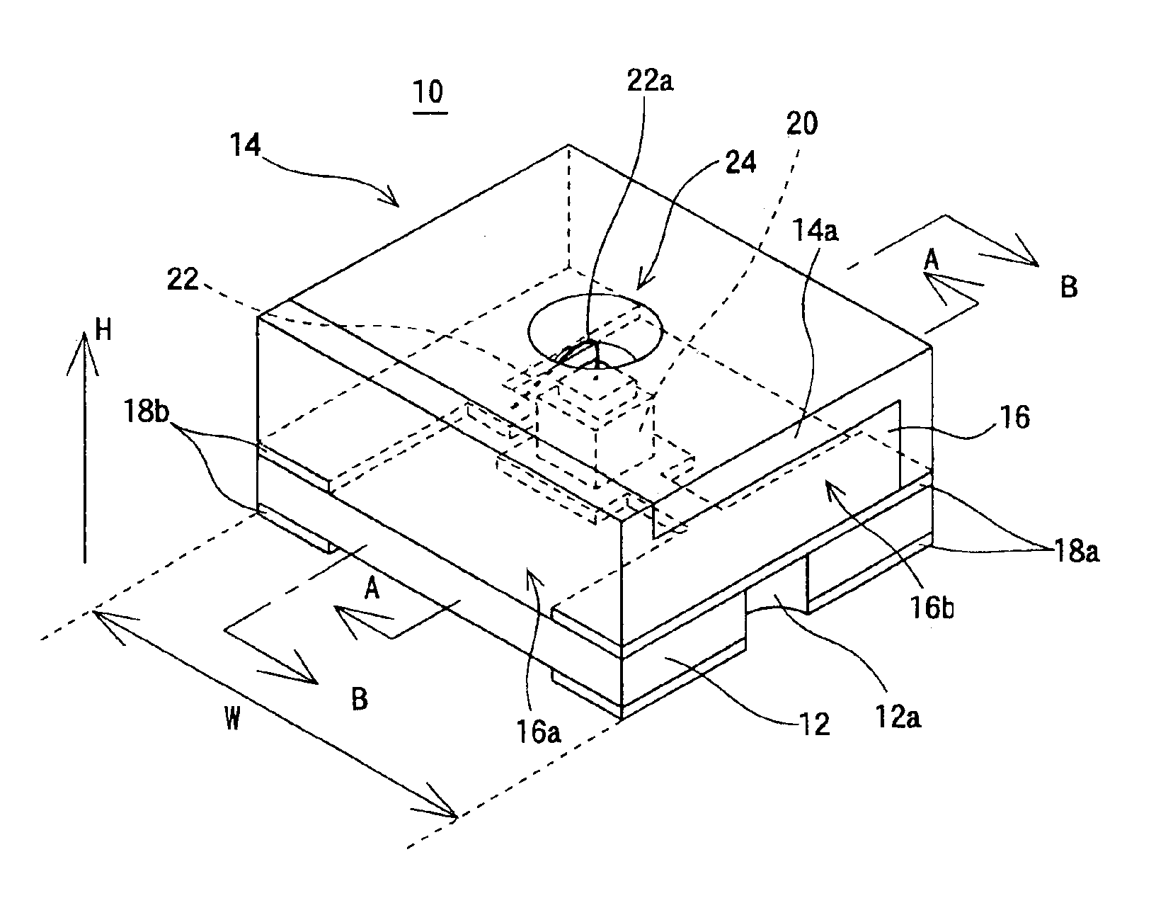
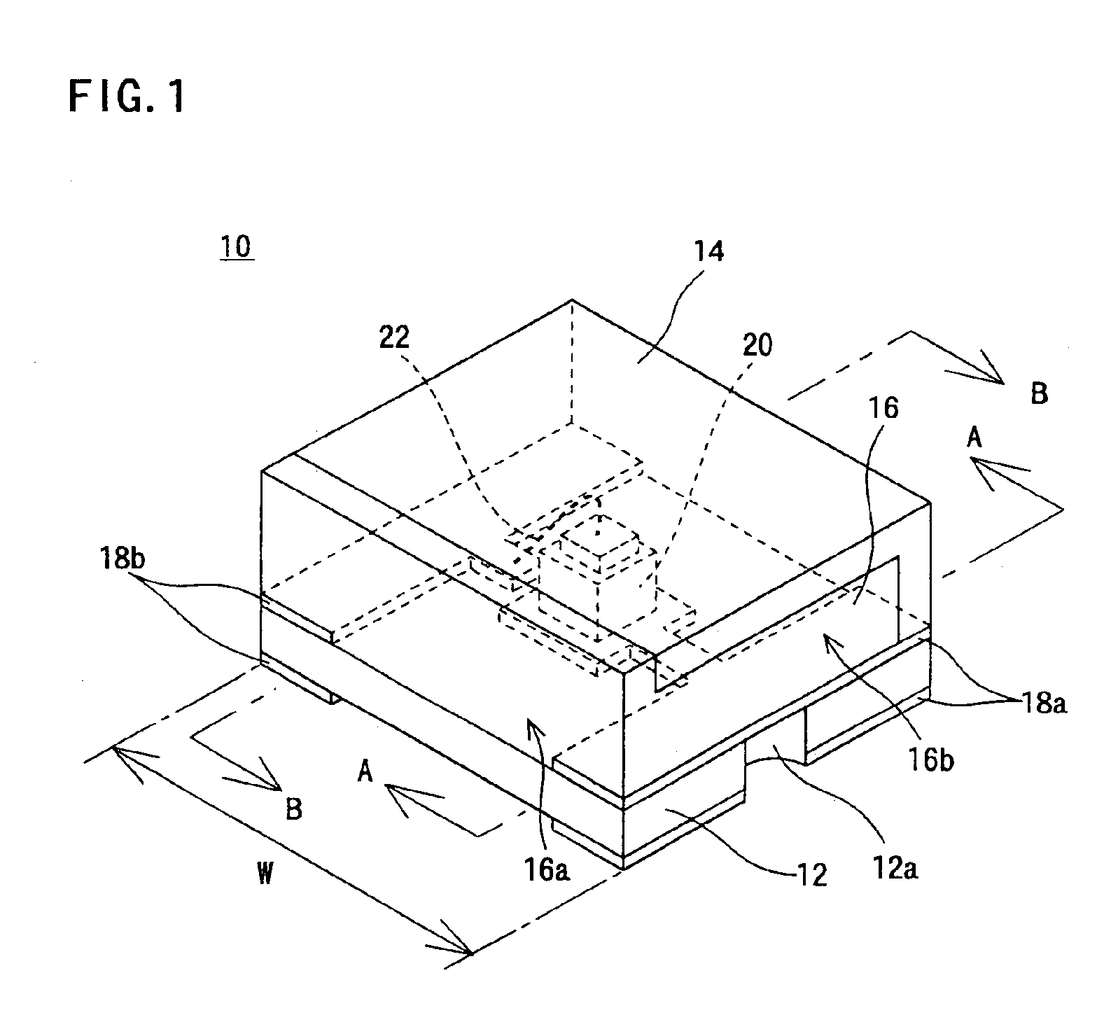
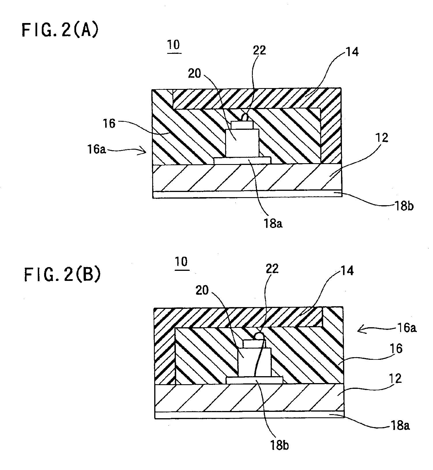
[0064]Referring to FIG. 1, a side-emission type semiconductor light-emitting device (hereinafter referred merely to as “light-emitting device”) 10 of this embodiment includes an insulating substrate (hereinafter referred merely to as “substrate”) 12 formed of a glass epoxy or the like. On the substrate 12, a reflector (case) 14 formed of a resin having opacity and reflectivity is provided. The substrate 12 is provided with electrodes 18a and 18b, and as can be understood from FIG. 2(A) of cross-sectional view at a line IIA—IIA in FIG. 1, a semiconductor light-emitting element (LED chip) 20 is die-bonded onto the electrode 18a by a DB paste (not shown). Meanwhile, as can be understood from FIG. 2(B) of a cross-sectional view at a line IIB—IIB in FIG. 1, the electrode 18b and the LED chip 20 are electrically connected with each other by a bonding wire 22 such as a gold wire and etc.

[0065]The electrode 18a is formed to extend from a front side to a...


PUM


Abstract

A side-emission type semiconductor light-emitting device 10 includes a substrate 12, and the substrate 12 is provided with a case 14 formed of a resin having opacity and reflectivity. The substrate 12 is formed, on its surface, with electrodes 18a and 18b onto which an LED chip 20 is bonded. A transparent or translucent resin 16 is charged between the substrate 12 and the case 14 whereby the LED chip 20 is molded. A light-emitting surface of the side-emission type semiconductor light-emitting device 10 includes surfaces 16a, 16b and a surface opposite to the surface 16b which are formed of the transparent or translucent resin 16. Furthermore, the light-emitting surface is formed by a roughened surface. Due to this, a light outputted from the LED chip and a light reflected from the case 14 is scattered by the light-emitting surface.

Description

CROSS-REFERENCE TO RELATED APPLICATIONS[0001]This application is a division of U.S. application Ser. No. 10 / 019,508, filed on Apr. 11, 2002, now abandoned, and entitled, “Side-Emission type Semiconductor Light-Emitting Device and Manufacturing Method Thereof”, the disclosure of which is incorporated herein by reference.TECHNICAL FIELD[0002]The present invention relates to a side-emission type semiconductor light-emitting device and a manufacturing method thereof. More specifically, the present invention relates to a side-emission type semiconductor light-emitting device in which an LED chip is bonded onto an electrode on a substrate, and a manufacturing method thereof.PRIOR ART[0003]An example of this kind of a conventional side-emission type semiconductor light-emitting device and a manufacturing method thereof is disclosed in a Japanese Patent Laying-open No.5-315651 (H01L 33 / 00) laid-open on Nov. 26, 1993. A side-emission type semiconductor light-emitting device 1 manufactured in...

Claims


Application Information

Patent Timeline
IPC IPC(8): H01L33/00H01L29/22H01L33/48H01L33/60H01L33/62
CPCH01L33/486H01L33/60H01L24/97H01L33/62H01L2224/45144H01L2924/12041H01L2924/01029H01L2224/48091H01L33/58H01L2924/00014H01L2924/00
Inventor FUJII, TAKEHIRO
Owner ROHM CO LTD
Why Eureka
Try Eureka