Quantum interference device, atomic oscillator, electronic device, and moving object

Active Publication Date: 2016-04-14
MICROCHIP TECH INC
View PDF1 Cites 6 Cited by
  • Summary
  • Abstract
  • Description
  • Claims
  • Application Information

AI Technical Summary

Benefits of technology

[0046]With this configuration, it is possible to provide the moving object in

Problems solved by technology

However, the atomic oscillator disclosed in JP-A-2014-17824

Method used


Image

  • Quantum interference device, atomic oscillator, electronic device, and moving object
  • Quantum interference device, atomic oscillator, electronic device, and moving object
  • Quantum interference device, atomic oscillator, electronic device, and moving object

Examples


first embodiment

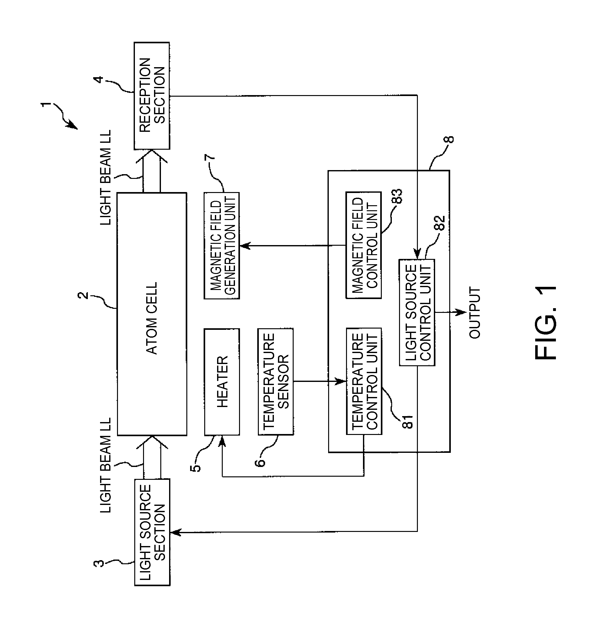
[0072]First, an atomic oscillator according to a first embodiment of the present disclosure is described.

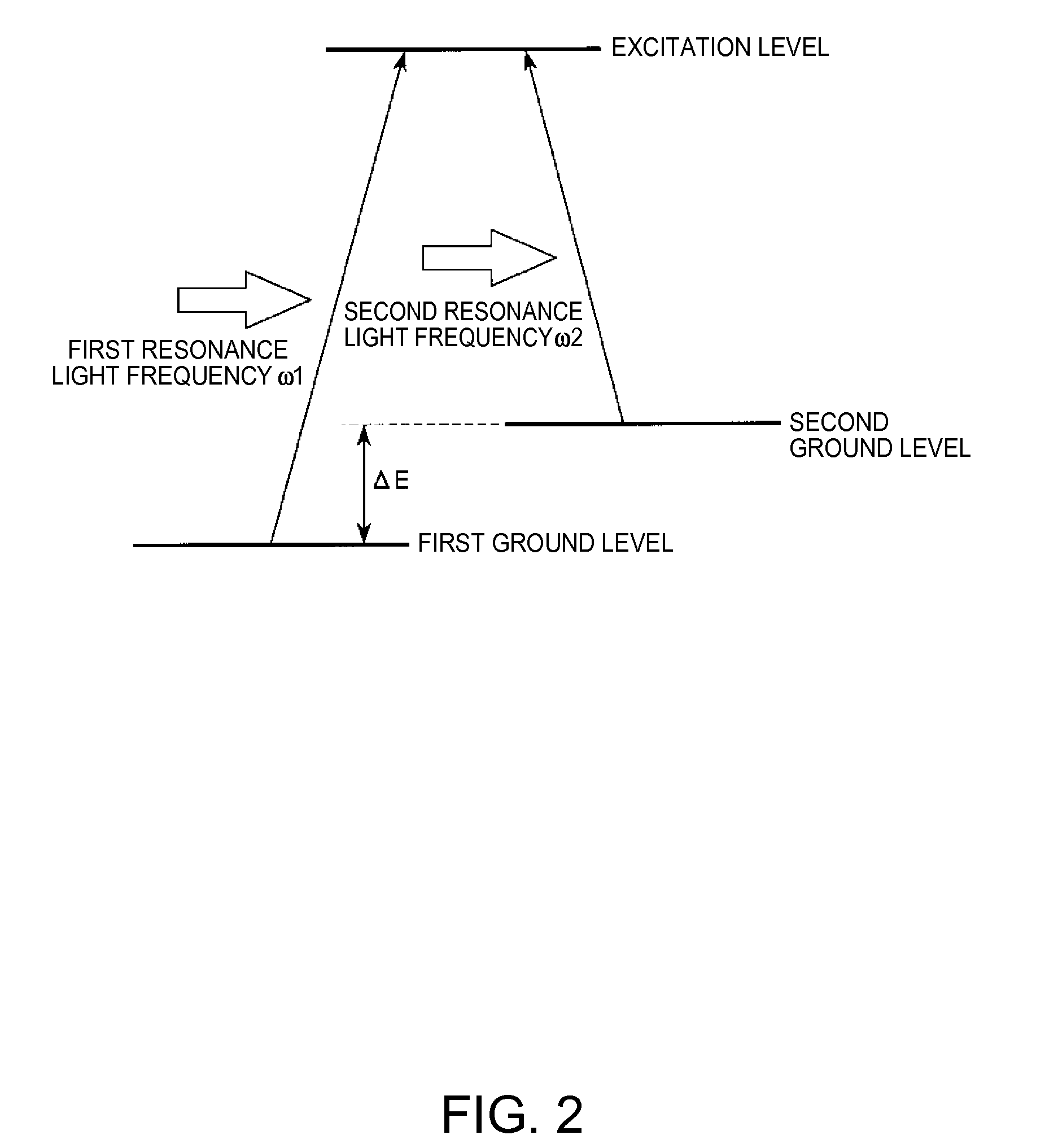
[0073]FIG. 1 is a schematic diagram illustrating the atomic oscillator (quantum interference device) according to the first embodiment of the present disclosure. FIG. 2 is a diagram schematically illustrating the energy state of alkali metal atoms. FIG. 3 is a graph illustrating the relationship between a frequency difference of two light beams emitted from a light source section and the intensity of light beam detected by a reception section.

[0074]With reference to FIG. 1, an atomic oscillator 1 uses quantum interference effects and includes an atom cell 2 (gas cell), a light source section 3, a reception section 4, a heater 5, a temperature sensor 6, a magnetic field generation unit 7, and a control unit 8.

[0075]First, the principle of the atomic oscillator 1 is described.

[0076]As shown in FIG. 1, in the atomic oscillator 1, the light source section 3 emits a light beam LL towa...

modification example

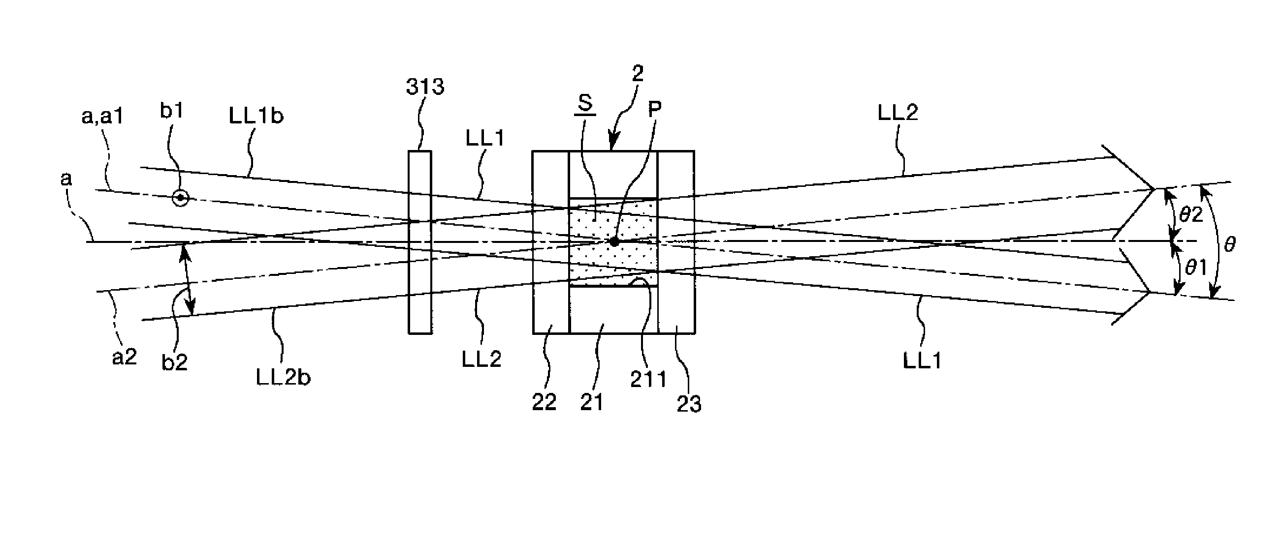
[0166]FIG. 11 is a diagram illustrating light beams respectively emitted from the first light source device and the second light source device of a light source section according to a modification example of the first embodiment of the present disclosure.

[0167]In the modification example shown in FIG. 11, in the atom cell 2, the optical axis a1 of the resonance light beam pair LL1 is offset with respect to the axis line “a” by an inclined angle θ1. In contrast, in the atom cell 2, the optical axis a2 of the adjustment light beam LL2 is offset with respect to the axis line “a” on the opposite side of the optical axis a1 by the inclined angle θ2. Therefore, it is possible to realize a configuration in which the symmetry of the axis line “a” is high.

[0168]Here, in the modification example shown in FIG. 11, similarly to the above-described example shown in FIG. 5, in the atom cell 2, the optical axis a1 of the resonance light beam pair LL1 is offset with respect to the optical axis a2 o...

second embodiment

[0170]Subsequently, a second embodiment of the present disclosure will be described.

[0171]FIG. 12 is a schematic diagram illustrating an atomic oscillator (quantum interference device) according to the second embodiment of the present disclosure. FIG. 13 is a diagram illustrating light beams respectively emitted from the first light source device and the second light source device of a light source section shown in FIG. 12.

[0172]This embodiment is the same as the first embodiment except that the configurations of the first light source device and the second light source device are different from those of the first embodiment and a λ / 4 wavelength plate and a polarizer are added between the atom cell and the reception section.

[0173]In the description below, the second embodiment will be described based on the difference from the above-described embodiment, and the same matters will not be repeated. In addition, in FIGS. 12 and 13, the same reference symbols are used for the same confi...


PUM


Abstract

An atomic oscillator includes an atom cell, a first light source device, a second light source device, and a reception section. The atom cell is filled with alkali metal. The first light source device emits a light beam that includes a resonance light beam pair configured to be circularly polarized with each other in the same direction and configured to cause the alkali metal to resonate. The second light source device emits a light beam that includes adjustment light beam configured to be circularly polarized in a reverse direction to the resonance light beam pair. The reception device receives the resonance light beam pair that pass through the atom cell. The adjustment light beam may include the resonance light beam that causes the alkali metal to resonate. In addition, the resonance light beam pair may be a line and the adjustment light beam is a line.

Description

BACKGROUND[0001]1. Technical Field[0002]The present disclosure relates to a quantum interference device, an atomic oscillator, an electronic device, and a moving object.[0003]2. Related Art[0004]As an oscillator, an atomic oscillator oscillates based on the transition of atomic energy of an alkali metal such as rubidium or cesium. The atomic oscillator may have highly accurate oscillation properties in the long term.[0005]Generally, the operational principle of the atomic oscillator may be classified as a method using double resonance phenomena due to light beams and microwaves. The atomic oscillator may also be classified as a method using quantum interference effects (coherent population trapping (CPT)) due to two types of light beams having different wavelengths. In the methods, it is possible to miniaturize the atomic oscillator using the quantum interference effects rather than the atomic oscillator using the double resonance phenomena. Accordingly, an atomic oscillator can be ...

Claims


Application Information

Patent Timeline
IPC IPC(8): H03B17/00
CPCH03B17/00H03L7/26G04F5/14G04F5/145H03L1/04
Inventor HAYASHI, NOBUHITOMAKI, YOSHIYUKI
Owner MICROCHIP TECH INC
Why Eureka
Try Eureka