
Organic electroluminescent display and manufacturing method thereof, electro-optic device and manufacturing method thereof, and electronic device

a technology of electroluminescent display and manufacturing method, applied in the direction of luminescent screen, discharge tube, identification means, etc., can solve problems such as common problems, and achieve the effect of extremely efficient manufacturing and extremely efficient manufacturing

Inactive Publication Date: 2005-07-19
ELEMENT CAPITAL COMMERCIAL CO PTE LTD
View PDF19 Cites 77 Cited by
  • Summary
  • Abstract
  • Description
  • Claims
  • Application Information

AI Technical Summary

Benefits of technology

[0007]The present invention has resulted due to such requirements, with the object of providing a method and an organic EL display construction whereby an organic EL display can be manufactured extremely efficiently, or a method and an electro-optic device construction whereby an electro-optic device can be manufactured extremely efficiently.
[0019]According to the present invention, since an organic EL display is manufactured by sticking together a circuit substrate in which microstructures are set, and an emissive substrate formed with an emissive layer and the like, there is the effect that the organic EL display can be manufactured extremely efficiently.
[0020]In particular, according to the third and fourth aspects, since the organic EL display can be continuously manufactured, a reduction in manufacturing cost can also be achieved.

Problems solved by technology

Furthermore, this type of problem is also a common problem for electro-optic devices other than organic EL displays.

Method used


Image

  • Organic electroluminescent display and manufacturing method thereof, electro-optic device and manufacturing method thereof, and electronic device
  • Organic electroluminescent display and manufacturing method thereof, electro-optic device and manufacturing method thereof, and electronic device
  • Organic electroluminescent display and manufacturing method thereof, electro-optic device and manufacturing method thereof, and electronic device

Examples


first example

Mobile Type Computer

[0049]At first is a description of an example for where an organic EL display panel according to the embodiments is applied to a mobile type personal computer. FIG. 5 is a perspective view illustrating the construction of this personal computer. In the figure, a personal computer 1100 comprises a main frame 1104 incorporating a key board 1102, and a display unit 1106. The display unit 1106 has an organic EL display panel 100.

second example

Portable Telephone

[0050]Next is a description of an example for where an organic EL display panel is applied to a display portion of a mobile telephone. FIG. 6 is a perspective view illustrating the construction of this mobile telephone. In the figure, a mobile telephone 1200 incorporates a plurality of operating buttons 1202 as well as, an earpiece 1204, a mouth piece 1206 and the abovementioned organic EL display panel 100.

third example

Digital Still Camera

[0051]Next is a description of a digital still camera which uses an organic EL display panel in a finder. FIG. 7 is perspective view illustrating the construction of this digital still camera, with connections for external equipment also shown simplified.

[0052]In contrast to a normal camera where the film is exposed by an optical image of a photographic subject, with the digital still camera 1300, the optical image of the photographic subject is photoelectrically converted by an imaging element such as a CCD (charged coupled device) to thereby produce an image signal. Here, the construction is such that the abovementioned organic EL display panel 100 is provided on a back face of a case 1302 of the digital still camera 1300, and display is performed based on the image signal from the CCD. Therefore the organic EL display panel 100 functions as a finder for displaying the photographic subject. Furthermore, on the viewing side (the rear face side in the figure) of ...


PUM


Abstract

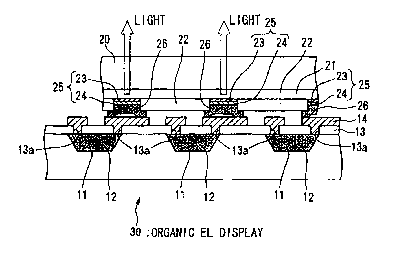
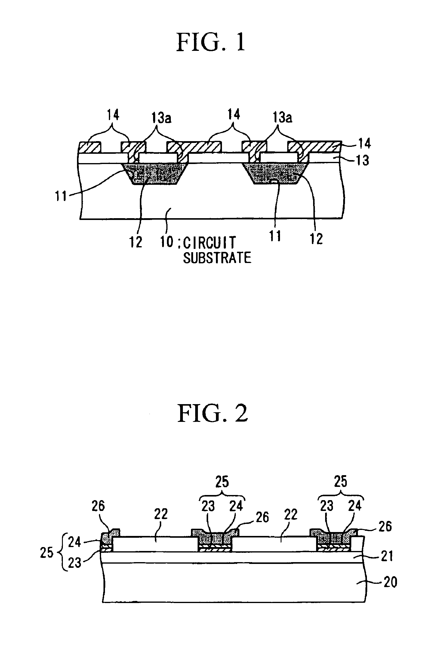
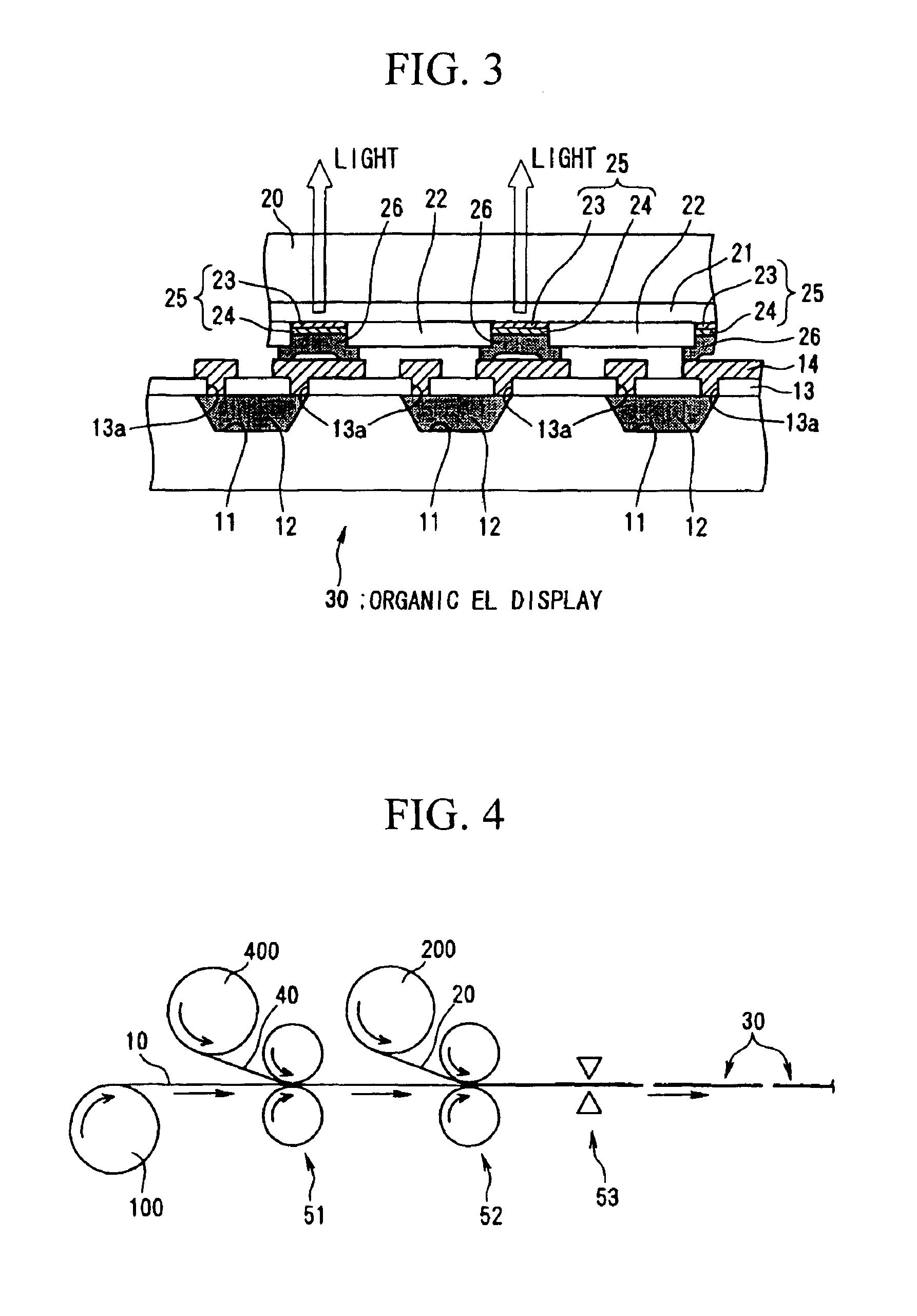
An object is to efficiently manufacture an organic EL display. A circuit substrate 10 in which is set microstructures 12 and which is formed with wiring 14, and a transparent substrate 20 formed with a transparent electrode 21, an emissive layer 25 and a cathode layer 26, are stuck together with the side formed with the wiring 14 and the side formed with the cathode layer 26 facing the inside, to thereby manufacture an organic EL display 30. In the sticking together of the circuit substrate 10 and the transparent substrate 20, an anisotropic conductive paste or an anisotropic conductive film can be used.

Description

BACKGROUND OF THE INVENTION[0001]1. Field of the Invention[0002]The present invention relates to the construction of an organic electroluminescent (hereunder EL for short) display and a manufacturing method thereof, to an electro-optic device and a manufacturing method thereof, and to an electronic device. In particular the invention is one where, in a manufacturing method for a display incorporating microstructures made with drive circuits for organic EL elements, the organic EL display can be manufactured extremely efficiently.[0003]2. Description of Related Art[0004]Heretofore, there is a method of manufacturing an electronic device using microstructures made with electronic circuit elements (refer for example to U.S. Pat. Nos. 5,904,545, 5,824,186, 5,783,856, and 5,545,291).[0005]That is, there is a manufacturing method which uses microstructures, and which enjoys for example the advantage that even with a configuration where a plurality of electronic circuits are scattered over...

Claims


Application Information

Patent Timeline
Patent Type & Authority Patents(United States)
IPC IPC(8): H01L27/32H01L27/28H01L51/52H01L51/50H05B33/10G09F9/00G09F9/30H01L51/56H05B33/22
CPCH01L27/3253H01L51/56H01L2251/5315H01L2251/566H10K59/1275H10K59/129H10K2102/3026H10K71/851H10K71/00
Inventor SHIMODA, TATSUYAMIYASHITA, SATORUINOUE, SATOSHI
Owner ELEMENT CAPITAL COMMERCIAL CO PTE LTD
Learn More