CMOS image sensor having row decoder capable of shutter timing control

a technology of image sensor and row decoder, which is applied in the field of semiconductor integrated circuits having row decoders capable of timing control, can solve the problem of invalid data of second frame data, and achieve the effect of substantially controlling exposure time without increasing the layout area

Inactive Publication Date: 2005-07-19
SAMSUNG ELECTRONICS CO LTD
View PDF7 Cites 30 Cited by
  • Summary
  • Abstract
  • Description
  • Claims
  • Application Information

AI Technical Summary

Benefits of technology

The technical effect of this patent is to offer a CMOS image sensor with a row decoder that controls exposure time effectively while keeping the size of the device small.

Problems solved by technology

The technical problem presented in this patent text relates to improving the performance of a complementary metal oxide semiconductor device (CMOS image sensor). More specifically, it describes issues related to the use of a traditional row decoder and how it affects the capture of image data. To solve these issues, a new method for controlling exposure time without adding more space requirements or complexity to the system, a new design has been developed.

Method used


Image

  • CMOS image sensor having row decoder capable of shutter timing control
  • CMOS image sensor having row decoder capable of shutter timing control
  • CMOS image sensor having row decoder capable of shutter timing control

Examples


Embodiment Construction

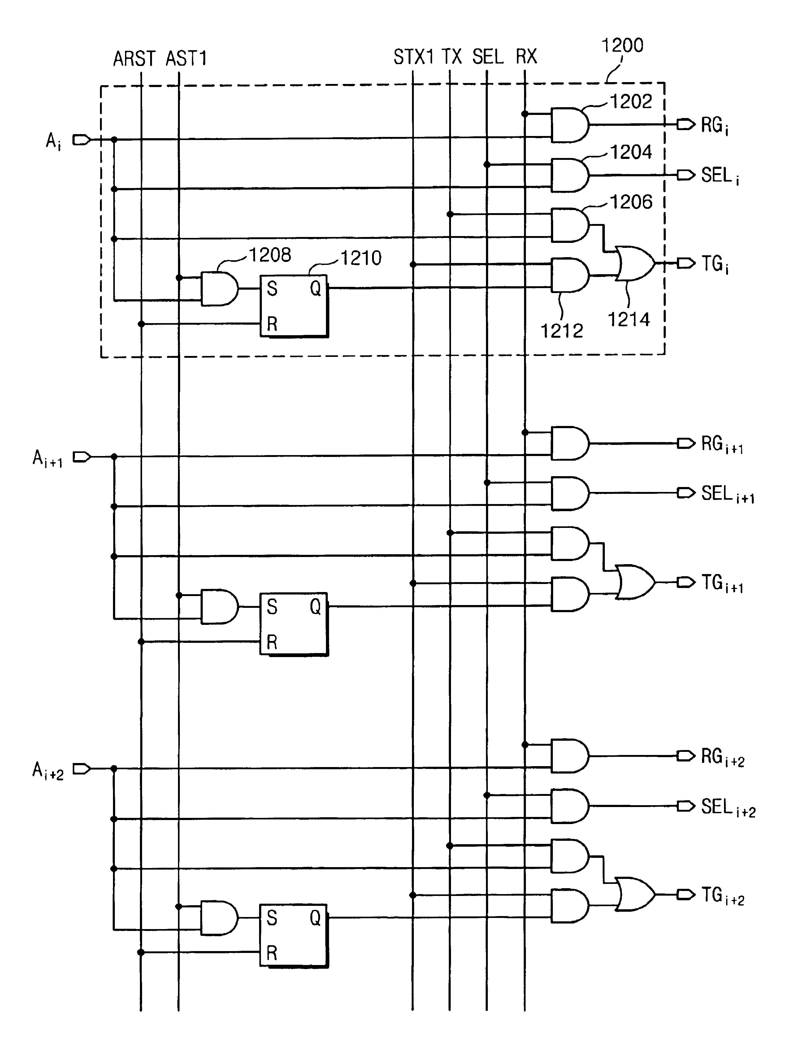
[0033]Reference will now be made in detail to preferred embodiments of the present invention, examples of which are illustrated in the accompanying drawings. However, it shall be understood that the present invention is not limited to the exemplary embodiments illustrated herein, and that the embodiments herein are rather introduced to provide easy and complete understanding of the scope and spirit of the present invention. To address the problems outlined in the Background section of the present disclosure, several non-preferred alternatives have been considered, as discussed with respect to FIGS. 9 through 11.

[0034]As shown in FIG. 9, a timing diagram is indicated generally by the reference numeral 900. Here, the row shutter value may be adjusted to prevent invalid data from being generated, so that the shutter row address of the second frame can be inputted in accordance with the last shutter row address of the first frame. Unfortunately, the method illustrated in FIG. 9 causes t...


PUM


Abstract

A CMOS image sensor having a row decoder capable of shutter timing control is provided, the row decoder addressing to a plurality of pixels arranged in rows and columns in a CMOS image sensor and including a plurality of unit arrays, wherein the unit arrays include a first NAND gate for generating a reset gate signal in response to an address signal and a reset signal, a second NAND gate for generating a selection gate signal in response to the address signal and a selection signal, a latch for resetting an output thereof in response to an address latch signal and latching the address signal as the output in response to the address latch signal and the address signal, a third NAND gate for receiving the address signal and a transmitted signal, a fourth NAND gate for receiving the output of the latch and a shutter transmitted signal, and an OR gate for receiving the outputs of the third and fourth NAND gates and generating a transmitted gate signal; wherein shuttering of a row address is latched in accordance with the blank interval of the horizontal synchronization signal using latches of the row decoder, and the shuttering operation is performed sequentially increasing the shuttering row address by 1, the invalid data that are not shuttered are thereby prevented from being generated though the row shutter value is changed suddenly.

Description


Claims


Application Information

Patent Timeline
Owner SAMSUNG ELECTRONICS CO LTD
Why Eureka
Try Eureka