Metal coordination compound, luminescence device and display apparatus

a technology of luminescence device and coordination compound, which is applied in the direction of discharge tube luminescence screen, thermoelectric device, organic chemistry, etc., can solve the problems of material change or life deterioration, material change or deactivation process, and the efficiency of luminescence is limited to at most 25%, and achieves high luminescence efficiency and high luminance

Inactive Publication Date: 2005-07-26
SAMSUNG ELECTRONICS CO LTD
View PDF8 Cites 1364 Cited by
  • Summary
  • Abstract
  • Description
  • Claims
  • Application Information

AI Technical Summary

Benefits of technology

[0035]Accordingly, principal objects of the present invention are to provide a luminescence material which exhibits a high luminescence efficiency and retains a high luminance for a long period, and also provide a luminescence device and a display apparatus using the same.

Problems solved by technology

Conventional organic EL devices have utilized fluorescence of which the luminescence efficiency is limited to at most 25%.
More specifically, because it is held in a high-energy excited state for a longer period, it is liable to react with surrounding materials and cause polymer formation among the excitons, thus incurring a higher probability of deactivation process resulting in a material change or life deterioration.

Method used


Image

  • Metal coordination compound, luminescence device and display apparatus
  • Metal coordination compound, luminescence device and display apparatus
  • Metal coordination compound, luminescence device and display apparatus

Examples


example 1

Synthesis of Example Compound No. 23

[0134]

[0135]In a 30 liter-three-necked flask, 307.3 g (960 mM) of 2-iodo-9,9-dimethylfluorene and 10 liters of dry THF (tetrahydrofuran) were placed and cooled to −72 to 70° C. under stirring in an argon gas stream atmosphere. To the mixture, a 1.6M solution of n-butyllithium in hexane was added dropwise in 1 hour, followed by further stirring for 2 hours at the temperature. Thereafter, under stirring at −73 to −71° C., to the system, a solution of 209.5 g (2016 mM) of trimethyl borate in 1.3 liters of dry THT was added dropwise in 2 hours. The reaction mixture was left standing overnight on an ice water bath. To the mixture, 1.6 liters of 4N-hydrochloric acid was added in 0.5 hour at 0-7° C., followed by stirring for 1 hour at room temperature and extraction with toluene. The organic layer was washed with saturated saline water, followed by distilling-off of the solvent under a reduced pressure to obtain a residue. To the residue, hexane was add...

example 2

Synthesis of Example Compound No. 43

[0140]

[0141]In a 100 ml-three-necked flask, 1.18 g (4.98 mM) of 2,5-dibromopyridine, 3.57 g (15.0 mM) 2-(9,9-dimethylfluorenyl)boronic acid prepared in Example 1, 10 ml of toluene, 5 ml of ethanol and 10 ml of 2M-sodium carbonate aqueous solution were placed and stirred at room temperature under nitrogen stream, and 0.35 g (0.30 mM) of tetrakis(triphenylphosphine)-palladium (0) was added thereto. Thereafter, reflux under stirring was performed for 12 hours under nitrogen stream. After completion of the reaction, the reaction product was cooled on an ice bath to precipitate a crystal, which was then filtered out and washed with water. To the crystal, 100 ml of methanol was added and washed at room temperature under stirring, and then was recovered by filtration. The resultant crystal was purified by silica gel column chromatography (eluent: chloroform) to obtain 2.10 g (yield=91.0%) of 2,5-bis{2-(9,9-dimethyl-fluorenyl)}pyridine (colorless crystal...

examples 3-11

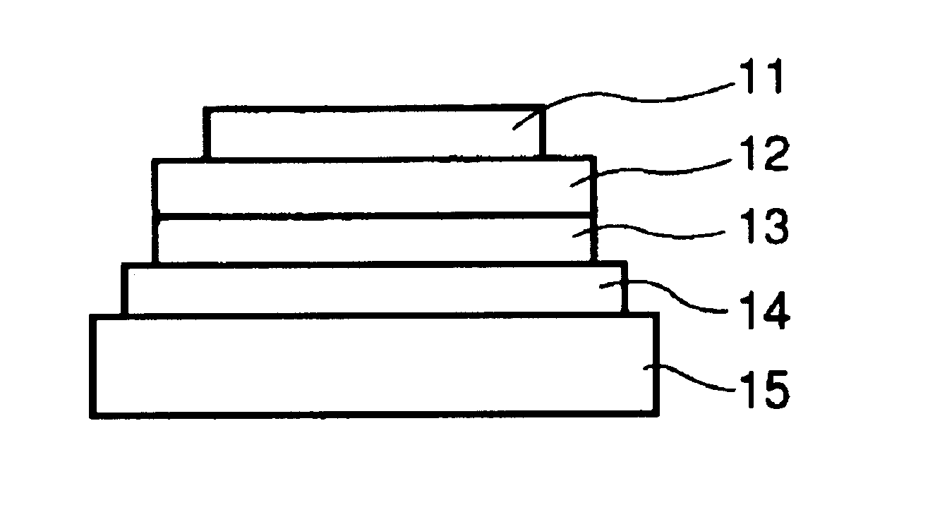
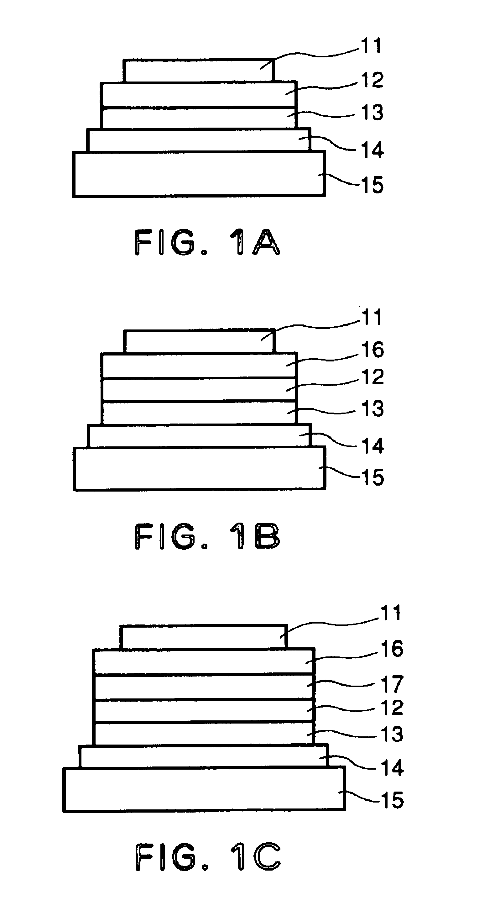
[0144]Each of luminescence devices having a layer structure shown in FIG. 1B were prepared in the following manner.

[0145]On a 1.1 mm-thick glass substrate (transparent substrate 15), a 100 nm-thick film (transparent electrode 14) of ITO (indium tin oxide) was formed by sputtering, followed by patterning to form a stripe electrode including 100 lines each having a width of 100 nm and a spacing with an adjacent line of 10 nm (i.e., electrode pitch of 110 nm).

[0146]On the ITO-formed substrate, three organic layers and two metal electrode layers shown below were successively formed by vacuum (vapor) deposition using resistance heating in a vacuum chamber (10−4 Pa).[0147]Organic layer 1 (hole transport layer 13) (40 nm): α-NPD[0148]Organic layer 2 (luminescence layer 12) (30 nm): co-deposited film of CBP:metal complex (metal coordination compound shown in Table 45) (95:5 by weight)[0149]Organic layer 3 (electron transport layer 16) (30 nm): Alq3[0150]Metal electrode layer 1 (metal electr...


PUM

PropertyMeasurementUnit
luminescence efficiencyaaaaaaaaaa
luminescenceaaaaaaaaaa
transparentaaaaaaaaaa

Abstract

An electroluminescence device having a layer containing a specific metal coordination compound is provided. The metal coordination compound is represented by formula (1) below:MLmL′n  (1), wherein M is a metal atom of Ir, Pt, Rh or Pd; L and L′ are mutually different bidentate ligands; m is 1, 2 or 3 and n is 0, 1 or 2 with the proviso that m+n is 2 or 3; a partial structure MLm is represented by formula (2) shown below and a partial structure ML′n is represented by formula (3) or (4) shown below:  at least one of the optional substituent(s) of the cyclic groups, and the cyclic groups CyC1 and CyC2 include an aromatic group capable of having a substituent represented by the following formula (5):  The metal coordination compound having the aromatic group is effective in providing high-efficiency luminescence and long-term high luminance.

Description

FIELD OF THE INVENTION AND RELATED ART[0002]The present invention relates to an organic luminescence device (also called an organic electroluminescence device or organic EL device) for use in a planar light source, a planar display, etc. Particularly, the present invention relates to a novel metal coordination compound and a luminescence device having a high luminescence efficiency and causing little change with time by using a metal coordination compound represented by formula (1) appearing hereinafter.[0003]An old example of organic luminescence device is, e.g., one using luminescence of a vacuum-deposited anthracene film (Thin Solid Films, 94 (1982) 171). In recent years, however, in view of advantages, such as easiness of providing a large-area device compared with an inorganic luminescence device, and possibility of realizing desired luminescence colors by development of various new materials and drivability at low voltages, an extensive study thereon for device formation as a ...

Claims


Application Information

Patent Timeline
Patent Type & Authority Patents(United States)
IPC IPC(8): C07F15/00H01L51/05H01L51/30H01L51/50C09K11/06H01L51/00
CPCC07F15/0033H01L51/0085H01L51/0059H01L51/0081H01L51/5012H10K85/631H10K85/324H10K85/342H10K50/11C09K11/06
Inventor TAKIGUCHI, TAKAOOKADA, SHINJIROTSUBOYAMA, AKIRAMIURA, SEISHIMORIYAMA, TAKASHIKAMATANI, JUNFURUGORI, MANABU
Owner SAMSUNG ELECTRONICS CO LTD
Why Eureka
Try Eureka