Semiconductor chip and conductive member for use in a light socket

Inactive Publication Date: 2005-08-16
JANNING JOHN L
View PDF8 Cites 59 Cited by
  • Summary
  • Abstract
  • Description
  • Claims
  • Application Information

AI Technical Summary

Benefits of technology

[0006]It is an object to impr

Problems solved by technology

A drawback with such light strings is that they commonly include of a plurality of individual light units with bulbs which are electrically connected in series and not in parallel.
As the bulb is used, over time, the filament will burn out, breaking the series circuit in which the

Method used


Image

  • Semiconductor chip and conductive member for use in a light socket
  • Semiconductor chip and conductive member for use in a light socket
  • Semiconductor chip and conductive member for use in a light socket

Examples


Embodiment Construction

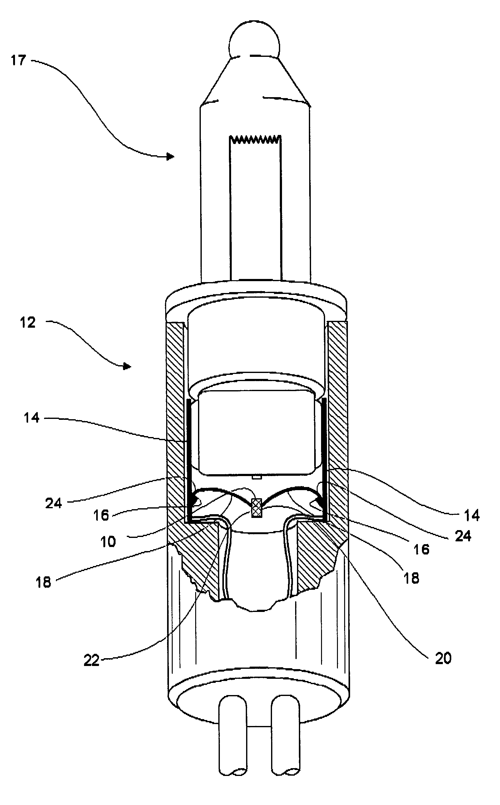
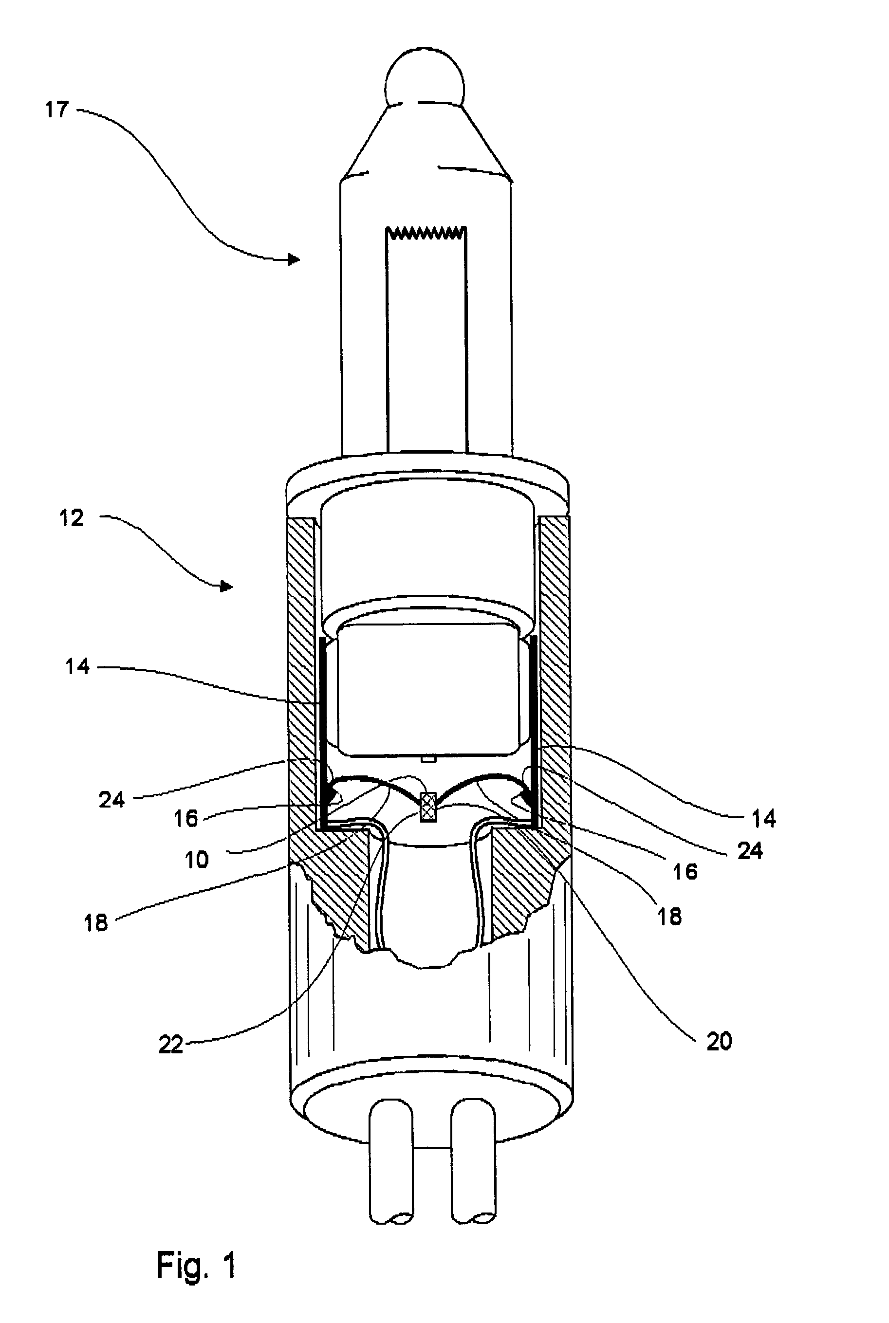
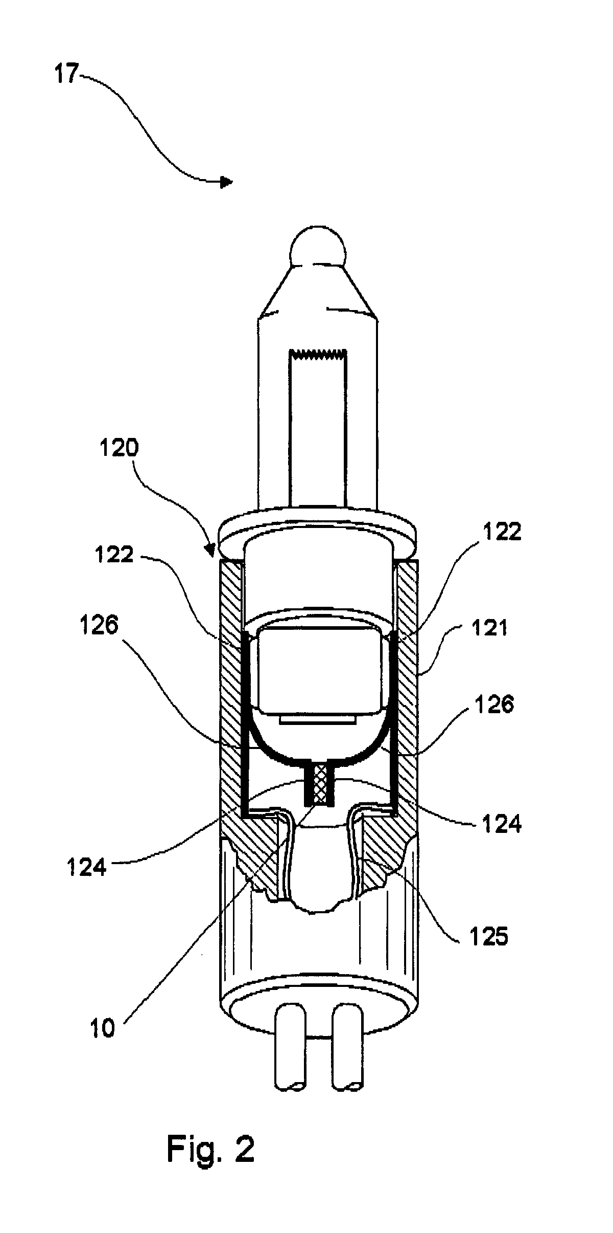
[0019]Referring now to the drawings, the semiconductor chip of the present invention is generally designated by the numeral 10. The semiconductor chip 10 is a relatively flat and thin plate which is of the type described in U.S. Provisional Patent Application No. 60 / 471,094. The chip 10 is used in various embodiments described herein.

[0020]FIG. 1 shows a modified light socket 12 having conductive terminals 14 on each side with plug-in socket surfaces 16 formed therein in a portion of each terminal 14 where a light bulb 17 normally seats when operatively disposed within the socket 12. The light bulb 17 has a pair of conductive leads which connect to a filament contained within a glass envelope. The chip 10 may include operatively connected conductive leads 18, wherein one lead 18 extends from each side 20 and 22 of the chip 10 and can be bonded thereto by a conductive epoxy, for example. A terminal end 24 of each lead 18 is configured to be operatively received into the plug-in socke...


PUM


Abstract

A shunt device for a light socket includes a semiconductor chip which is operably interposed between a pair of electric terminals of the socket. The sockets are in series for a conventional set of display lights, such as holiday lights.

Description

FIELD OF INVENTION[0001]The present invention relates to a lamp socket for light strings having lights arranged in series. More particularly, the invention relates to a semiconductor chip and conductive member for use in a light socket forming a shunt to allow for electricity to continually conduct throughout the light string keeping the remainder of the lights lit when one or more lights on the string burn out, become dysfunctional or are removed from a socket.BACKGROUND OF THE INVENTION[0002]Decorative light strings which are connected in series are highly popular in the United States, especially during holidays in November and December. A drawback with such light strings is that they commonly include of a plurality of individual light units with bulbs which are electrically connected in series and not in parallel. The bulbs are typically incandescent bulbs having a filament formed between two leads of the bulb, the filament giving off light when a current is passed from one lead ...

Claims


Application Information

Patent Timeline
IPC IPC(8): H05B39/10H05B39/00F21V19/00H01R13/66H01R33/09
CPCH05B39/105F21V19/0005H01R13/665H01R33/09
Inventor JANNING, JOHN L.
Owner JANNING JOHN L
Why Eureka
Try Eureka