Planar lightwave circuit and optical circuit

a lightwave circuit and optical circuit technology, applied in the field of planar lightwave circuits, can solve the problems of superhigh-speed coupling loss, large waveguide, accumulation of coupling loss, etc., and achieve the effect of suppressing coupling loss

Inactive Publication Date: 2005-08-30
NIPPON TELEGRAPH & TELEPHONE CORP
View PDF21 Cites 23 Cited by
  • Summary
  • Abstract
  • Description
  • Claims
  • Application Information

AI Technical Summary

Benefits of technology

[0014]It is an object of the present invention to provide a planar lightwave circuit which can suppress the coupling loss while downsizing is realized.

Problems solved by technology

However, there is a problem in that the coupling loss of the superhigh- waveguide is very large.
The coupling loss occurs when connecting different types of waveguides The coupling loss occurs due to difference of field distribution between the different types of waveguides, and the coupling loss accumulates as connecting points increases.
That is, although the circuit can be downsized by increasing , the coupling loss increases.
Therefore, construction of a practical system has limitations That is, it becomes difficult to enlarge capacity of transmission lines unless the coupling loss of the superhigh- waveguide is decreased, so that functions and scale of the optical communication system may be limited.
However, it is known that the coupling loss for the narrow taper spotsize converter largely changes due to slight fabrication error of core width, and the like.
Thus, the narrow taper spotsize converter has not been in practical use.

Method used


Image

  • Planar lightwave circuit and optical circuit
  • Planar lightwave circuit and optical circuit
  • Planar lightwave circuit and optical circuit

Examples


first embodiment

[First Embodiment]

FIRST EXAMPLE

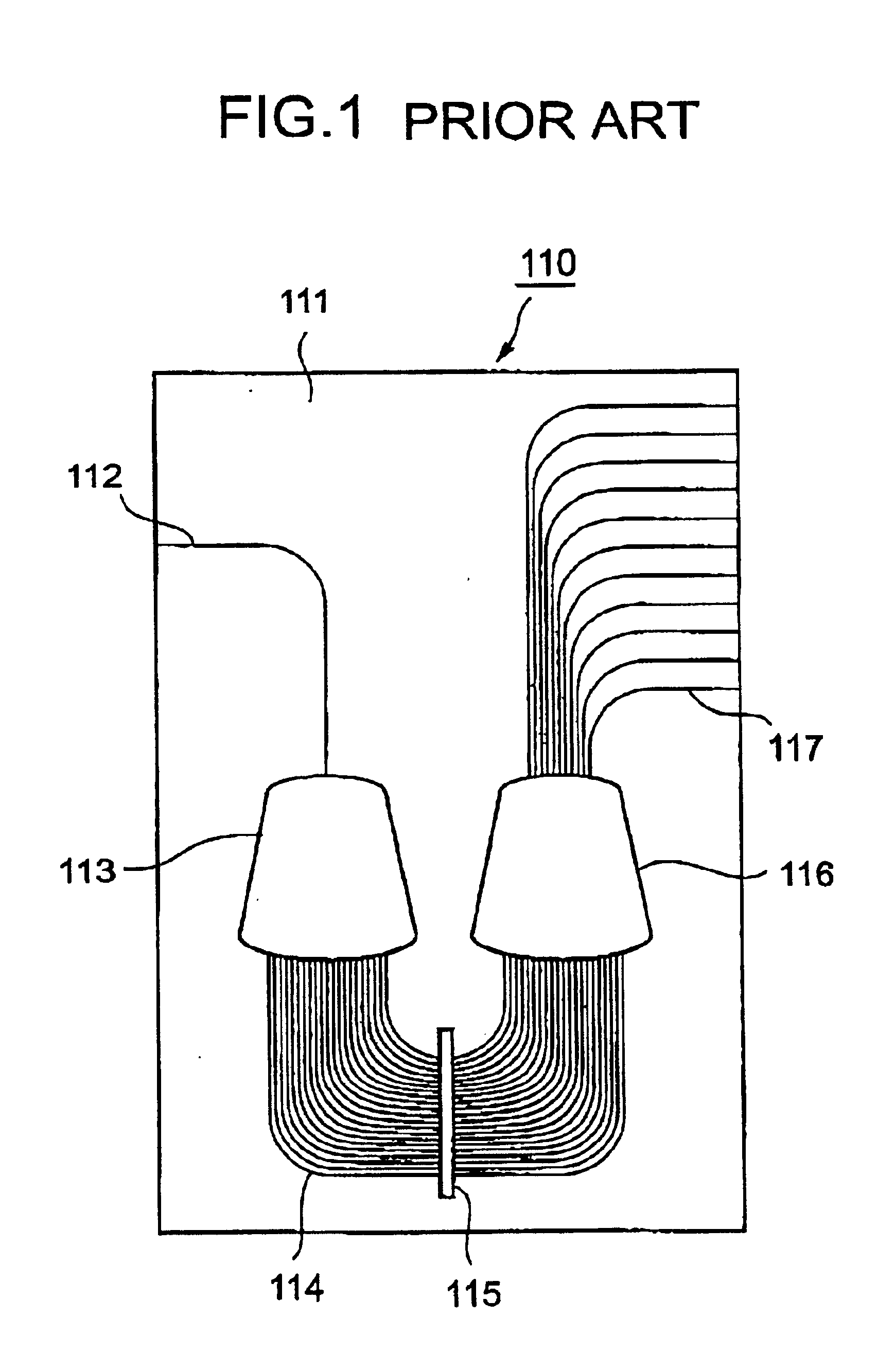
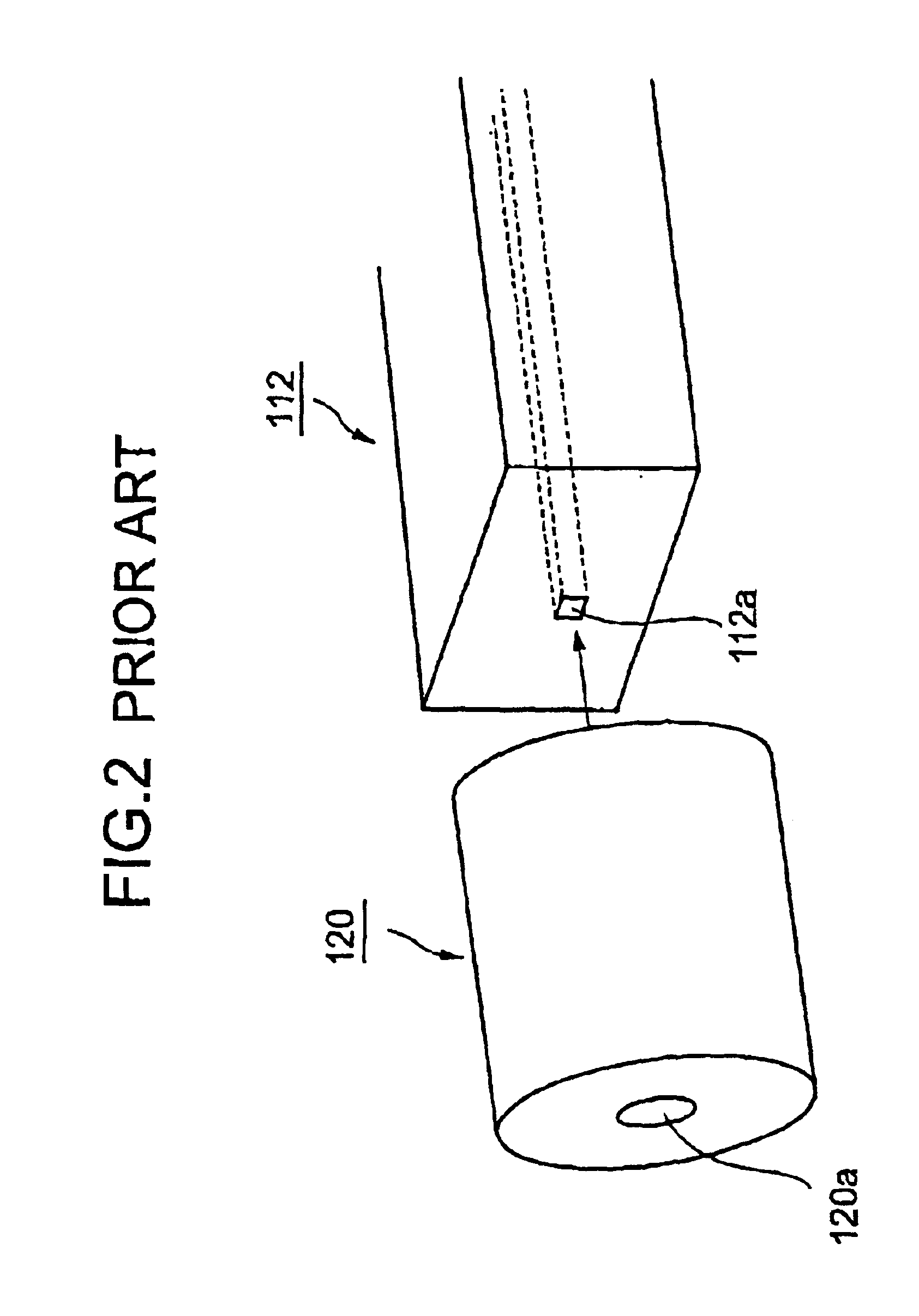
[0104]The first example of the first embodiment of the planar lightwave circuit of the present invention will be described with reference to FIGS. 4-8. FIG. 4 is a schematic block diagram of the planar lightwave circuit, FIG. 5 is a magnified view of the core of the input waveguide and the output waveguide of the planar lightwave circuit of FIG. 4. FIGS. 6A-6E are diagrams for explaining a process for fabricating the input waveguide and the output waveguide of the planar lightwave circuit of FIG. 4. FIG. 7 shows a relationship between the core width and the coupling loss of the end face of the substrate which is obtained by calculation. FIG. 8 is a diagram for explaining dicing error.

[0105]As shown in FIG. 4, an input waveguide 12 made of silica-based glass is formed on a substrate 11 made of silicon in which the input waveguide 12 includes a core having high refractive index and a cladding having low refractive index, and the core is covered by the cl...

second embodiment

[Second embodiment]

FIRST EXAMPLE

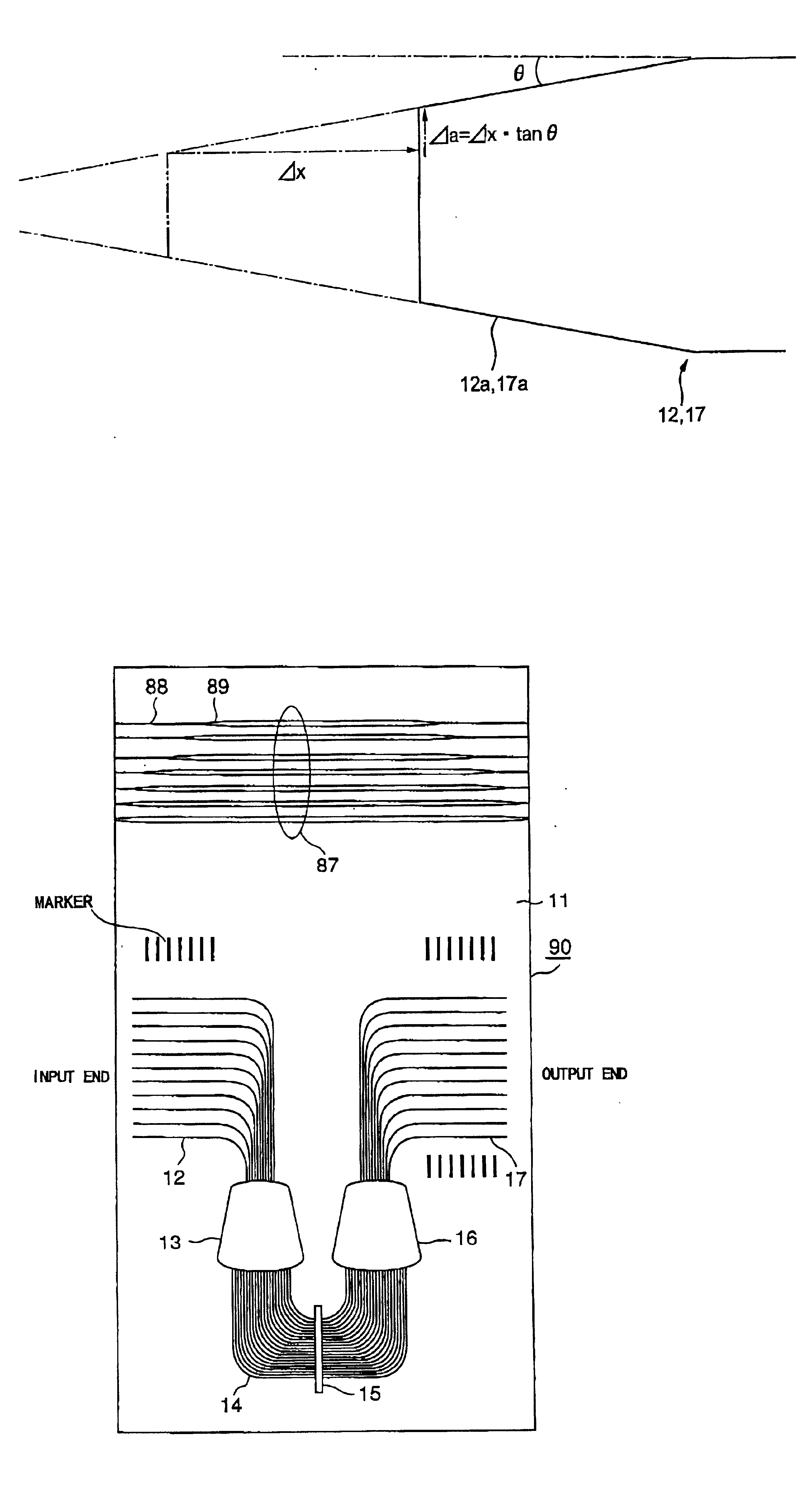
[0134]A first example of the second embodiment will be described with reference to FIGS. 12 and 13. FIG. 12 shows a schematic block diagram of the planar lightwave circuit, FIG. 13 shows a magnified view of the core of the input waveguides or the output waveguides. Parts which are the same as those of the first embodiment are not described, and the same symbols as those used in the first embodiment are used.

[0135]In this embodiment, the present invention is applied to an arrayed waveguide grating (AWG), which is one of planar lightwave circuits, which performs multiplexing of optical signals of a plurality of different wavelengths and demultiplexing in an wavelength division multiplexing communication system. AWG is an example of a waveguide type optical circuit.

[0136]As shown in FIG. 12, a plurality of input waveguides 12 are provided on the substrate 11. The core width of input end face of the taper part 12aa of the core 12a is different by each inp...

second example

[0143]It is also possible to apply the core 32a, 37a of the second example of the first embodiment to this embodiment, in which a plurality of steps 32aa, 37aa are formed such that the core width decreases gradually toward the end side of input or output.


PUM


Abstract

A planar lightwave circuit is provided. The planar lightwave circuit includes a waveguide and a spotsize converter which is a part of the waveguide, wherein a core is embedded in a cladding in the waveguide, and the spotsize converter is located near an end face of a substrate on which the planar lightwave circuit is formed, the spotsize converter including: a core width fine-tuning part in an end face side of the substrate; and a core width converting part which follows the core width fine-tuning part; wherein core width of the spotsize converter is minimum at an end face of the substrate, a mean taper angle θ1 of the core width fine-tuning part is larger than 0° and smaller than a mean taper angle θ2 of the core width converting part.

Description

BACKGROUND OF THE INVENTION[0001]1. Field of the Invention[0002]The present invention relates to a planar lightwave circuit (PLC) which can decrease the coupling loss between a planar lightwave circuit and an optical fiber or between planar lightwave circuits.[0003]2. Description of the Related Art[0004]It is predicted that the planar lightwave circuits will be used more and more as main parts which have important functions such as routing of an optical signal in superfast large-capacity optical communication systems from now on. Especially, it is required to construct a larger optical communication system as capacity required for communication increases. In order to realize the enlargement of the optical communication system, it is necessary to downsize the planar lightwave circuit and to allow connection between many planar lightwave circuits.[0005]FIG. 1 is a schematic diagram of structure of a conventional planar lightwave circuit. As shown in FIG. 1, an input waveguide 112 is f...

Claims


Application Information

Patent Timeline
Patent Type & Authority Patents(United States)
IPC IPC(8): G02B6/13G02B6/132G02B6/122G02B6/136G02B6/12G02B6/34
CPCG02B6/12011G02B6/12016G02B6/12023G02B6/1228G02B6/132G02B6/136G02B2006/121G02B2006/12176
Inventor MIZUNO, TAKAYUKIKITOH, TSUTOMUINOUE, YASUYUKIHIBINO, YOSHINORIITOH, MIKITAKASAIDA, TAKASHIHIDA, YASUHIRO
Owner NIPPON TELEGRAPH & TELEPHONE CORP
Why Eureka
Try Eureka