Planar magnetic field probe

a magnetic field and probe technology, applied in the direction of magnetic measurement, instruments, measurement devices, etc., can solve the problem of difficult to measure trace currents by the same magnetic field probe, and achieve the effect of accurate measurement of the magnetic field of a signal line, suppressing electric field coupling, and reducing the magnetic field

Inactive Publication Date: 2013-11-05
TATUNG COMPANY
View PDF7 Cites 13 Cited by
  • Summary
  • Abstract
  • Description
  • Claims
  • Application Information

AI Technical Summary

Benefits of technology

[0009]The invention is related to a planar magnetic field probe which can accurately measure the magnetic field of a signal line by reducing the magnetic field generated by the current of a ground layer on a circuit board, suppressing electric field coupling, and improving its sensitivity.
[0020]According to the above descriptions, a left multi-induction loop and a right multi-induction loop formed by the first patterned induction metal layer and the second patterned induction metal layer are used to increase sensitivity of detecting the magnetic field intensity, and a symmetrical shielded metal structure formed by the first patterned shielding metal layer and the second patterned shielding metal layer is used to surround the left multi-induction loop and the right multi-induction loop to reduce the electric field noise coupling. In this way, the sensitivity of the magnetic field intensity detection is increased and the electric field coupling is suppressed.

Problems solved by technology

Therefore it is difficult to measure trace currents by the same magnetic field probe that is used for the ground layer current.

Method used


Image

  • Planar magnetic field probe
  • Planar magnetic field probe
  • Planar magnetic field probe

Examples


Embodiment Construction

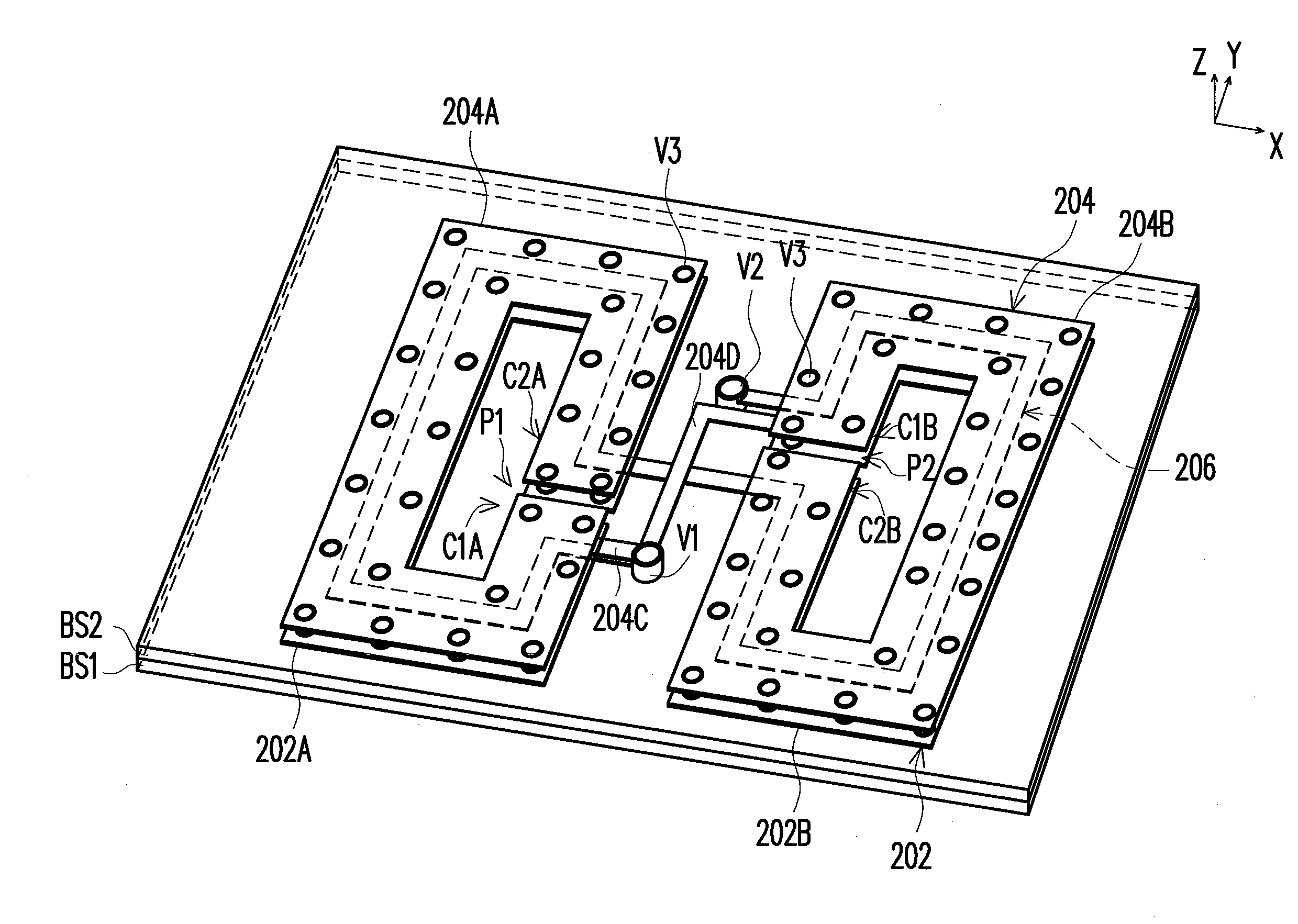
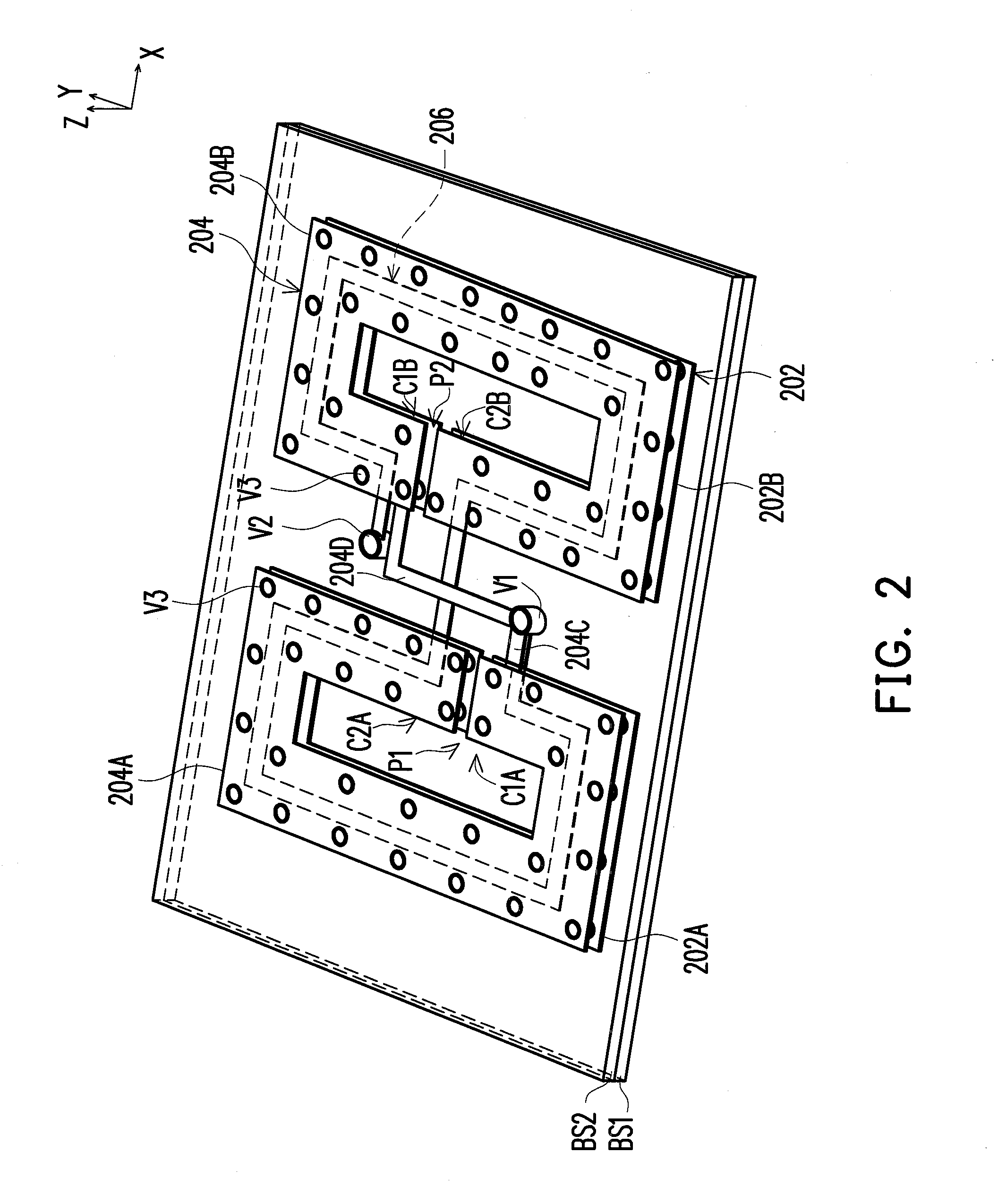
[0027]FIG. 2 is a schematic diagram of a planar magnetic field probe according to an embodiment of the invention. Referring to FIG. 2, the planar magnetic field probe 200 is fabricated on a multi-layer printed circuit board. In the present embodiment, the planar magnetic field probe 200 includes a first substrate BS1, a second substrate BS2, a first through via V1, a second through via V2, and a plurality of third through vias V3 penetrating through the first substrate BS1 and the second substrate BS2, where the first substrate BS1 and the second substrate BS2 are, for example, made of fibreglass. A first patterned shielding metal layer 202 and a second patterned shielding metal layer 204 are respectively formed on the outer sides of the first substrate BS1 and the second substrate BS2, and a first patterned induction metal layer 206 is formed between the first substrate BS1 and the second substrate BS2.

[0028]The structure of first patterned induction metal layer 206 is shown in FIG...


PUM


Abstract

A planar magnetic field probe is provided. The planar magnetic field probe increases the sensitivity of magnetic field intensity detection by using a left multi-sensor loop and a right multi-sensor loop formed by a first patterned metal layer and a second patterned metal layer, and decreases the electric field noise coupling by surrounding the left multi-sensor loop and the right multi-sensor loop with a symmetrical shielding metal structure formed by a first patterned shielding metal layer, a second patterned shielding metal layer and a plurality of through vias.

Description

CROSS-REFERENCE TO RELATED APPLICATION[0001]This application claims the priority benefit of Taiwan application serial no. 100102043, filed Jan. 20, 2011. The entirety of the above-mentioned patent application is hereby incorporated by reference herein and made a part of this specification.BACKGROUND[0002]1. Field of the Invention[0003]The invention relates to a planar magnetic field probe. Particularly, the invention relates to a planar magnetic field probe capable of suppressing electric field coupling and having high sensitivity.[0004]2. Description of Related Art[0005]A near-field magnetic field probe is generally designed as a handheld device, which can be used to measure electromagnetic radiation of an electronic device, or used to position a possible electromagnetic radiation source of the electronic devices.[0006]The magnetic field probe is generally made in the form of a loop. The probe is connected to a measuring instrument (an oscilloscope or a spectrum analyser, etc.) thr...

Claims


Application Information

Patent Timeline
Patent Type & Authority Patents(United States)
IPC IPC(8): G01R33/02
CPCG01R33/0283
Inventor CHAO, SHIH-CHIEHHUANG, CHIH-WEN
Owner TATUNG COMPANY
Why Eureka
Try Eureka