System and method of processing a data signal

a data signal and data processing technology, applied in the direction of noise figure or signal-to-noise ratio measurement, instruments, transmission monitoring, etc., can solve the problems of random jitter, bit error, and inability to reliably test duts at frequencies over 1.0625 gbps, so as to reduce or eliminate jitter from serial encoded data

Inactive Publication Date: 2005-08-30
II VI DELAWARE INC
View PDF5 Cites 66 Cited by
  • Summary
  • Abstract
  • Description
  • Claims
  • Application Information

AI Technical Summary

Benefits of technology

[0014]The present invention provides a system and method for reducing or eliminating jitter from serial encoded data produced by a SERDES. In particular, the present invention includes a system and method for processing a data signal. This system and method includes a first circuit or set of steps configured to generate a first data signal based on a pattern. The first data signal including variations from the pattern and being transmitted at a first frequency. Also included is a second circuit or set of steps configured to generate a second data signal by delaying the first data signal by a first amount of time that is subject to a series of adjustments. The system and method further includes a third circuit or set of steps configured to latch states of the second data signal. Also included is a fourth circuit or set of steps configured to take measurements of the variations from the pattern by reference to the states of the second data signal following each adjustment in the series of adjustments. Finally, the system and method further includes a fifth circuit or set of steps configured to receive the measurements of the variations from the pattern from the fourth circuit or set of steps. The fifth circuit is (or the fifth steps are) configured to control the series of adjustments so that a measurement of a first spike of the variations is received from the fourth circuit or set of steps (the first spike corresponding to a first delay), control the series of adjustments so that a measurement of a second spike of the variations is also received from the fourth circuit or set of steps (the second spike corresponding to a second delay), and set the first amount of time to a third delay derived from the first delay and the second delay.

Problems solved by technology

Because of jitter typically included in data signals transmitted by a SERDES, testing DUTs at frequencies that exceed 1.0625 Gbps may not be reliable.
Random jitter is typically caused by thermal (or other random) noise effects of a system that affect the phase of the clock and / or data signals.
As a result, the data signal may not cross the reference value in time for the device to properly determine the intended state of the sample.
When this occurs, a bit error occurs.
The DUT may, therefore, fail a jitter test because of jitter present in a data signal transmitted to the DUT by a SERDES.
Similarly, a DUT may fail a bit error rate test due entirely to the jitter introduced by the SERDES into the data signal used to test the DUT.

Method used


Image

  • System and method of processing a data signal
  • System and method of processing a data signal
  • System and method of processing a data signal

Examples


Embodiment Construction

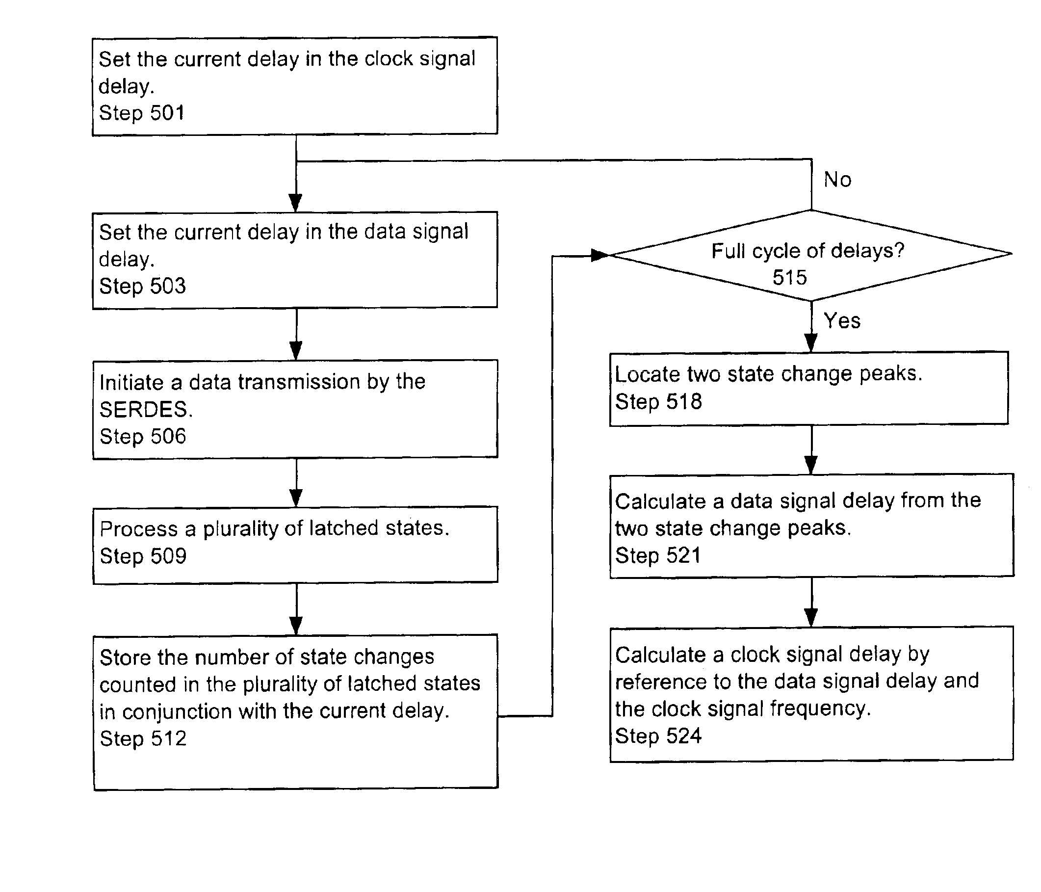
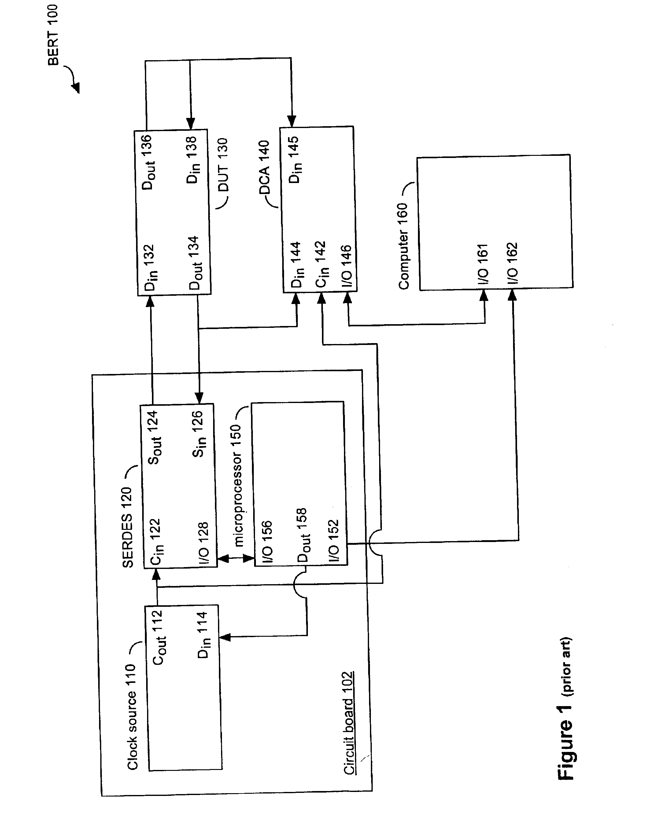
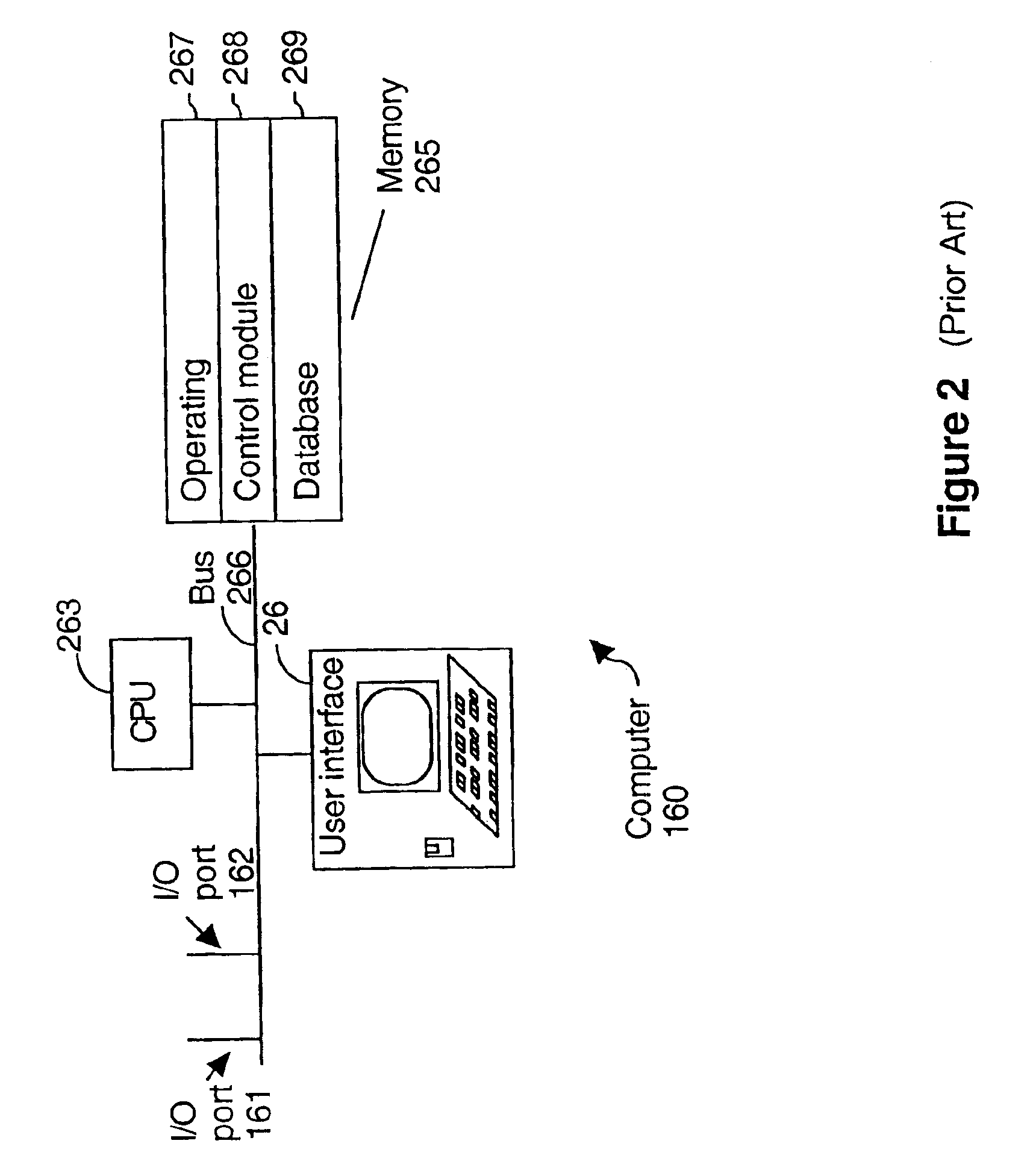
[0030]Referring to FIG. 1, there is shown a prior art BERT 100 for testing a DUT 130. As illustrated in FIG. 1, BERT 100 includes a circuit board 102, a clock source 110, a SERDES 120, a digital communication analyzer (“DCA”) 140, a microprocessor 150, and a computer 160.

[0031]The circuit board 102 typically comprises an insulated board on which interconnected circuits and components (e.g., the clock source 110 and the SERDES 120) are mounted. The circuit board 102 typically provides power and ground connections for the various components mounted thereon.

[0032]The clock source 110 is designed to provide a clock signal at a desired frequency. The clock source 110 may comprise a single, self contained circuit (e.g., an AMPTRON® or Cardinal Components, Inc. crystal based oscillator). Such circuits are preferably single frequency circuits, but the clock source 110 may also have multiple-frequency capability. If so, the microprocessor 150 or a user may select, through a plurality of pins...


PUM


Abstract

Systems and methods for testing bit processing capacities of electronic devices and for reducing or eliminating jitter that compromises the ability of electronic devices to perform this task. Embodiments include circuitry and a methodology for locating and employing a data signal delay—in conjunction with a latch—to reduce or eliminate jitter from serial encoded data generated by a serializer/deserializer. The data signal delay ensures that the latch latches a state of the serial encoded data at a position within a data signal cycle of minimum jitter.

Description

[0001]The present invention relates generally to an improvement in the ability of test systems to test bit processing capacities of electronic devices, and in particular to the elimination of jitter that compromises the ability of these systems to perform this task.BACKGROUND OF THE INVENTION[0002]A bit error rate (“BER”) is a ratio of bits received, processed, and / or transmitted with errors to a total number of bits received, processed, and / or transmitted over a given period of time. A BER is typically expressed as ten to a negative power. If, for example, a transmission comprises 1 million bits and one of these bits is in error (e.g., a bit is a first logic state instead of a second logic state), the transmission has a BER of 10−6. The BER is useful because it may characterize the ability of a device to receive, process, and / or transmit bits.[0003]Many devices are designed to receive, process, and then transmit a plurality of bits. An optoelectronic transceiver, for example, typic...

Claims


Application Information

Patent Timeline
Patent Type & Authority Patents(United States)
IPC IPC(8): G06F19/00G01R31/317
CPCG01R31/31709G01R31/3171
Inventor FISHMAN, ALEXHARITOS, KONSTANTINOS G.SUNG, PAULBANNIKOV, DMITRIDOROFEEV, SERGUEI
Owner II VI DELAWARE INC
Why Eureka
Try Eureka