Electronic component mounting method

a technology for mounting methods and components, applied in the direction of instruments, manufacturing tools, semiconductor/solid-state device details, etc., can solve the problems of reducing the pitch of the connecting portion, the actual position of the bg connecting portion is uncertain, and the mounting method and manufacturing method itself are difficult to achieve, so as to achieve more reliable solder bump component mounting

Inactive Publication Date: 2005-09-06
PANASONIC CORP
View PDF23 Cites 43 Cited by
  • Summary
  • Abstract
  • Description
  • Claims
  • Application Information

AI Technical Summary

Benefits of technology

[0068]By executing the first recognizing process for recognizing the reference mark provided on the electronic component to be mounted, the second recognizing process for recognizing the recognition mark of the target mounting position on th...

Problems solved by technology

However, on increasing the density, the lead pitch of the connecting portions has been reduced in stages, for example, from 0.5 mm through 0.3 mm to the extent of 0.2 mm, for which the mounting method and manufacturing method themselves have become hard to be achieved.
However, according to the mounting method and apparatus of the component having solder bumps constructed as above, the actual positions of the BG connecting portions become uncertain in the case of only the contour, or much time is required in executing the positional detection of the BG connecting portions one by one.
Therefore, the positional detection has been partially executed instead of executing the positional detection of all the BG connecting portions, meaning that the processing has been executed without...

Method used


Image

  • Electronic component mounting method
  • Electronic component mounting method
  • Electronic component mounting method

Examples


first embodiment

[0107]the present invention will be described in detail below with reference to the drawings.

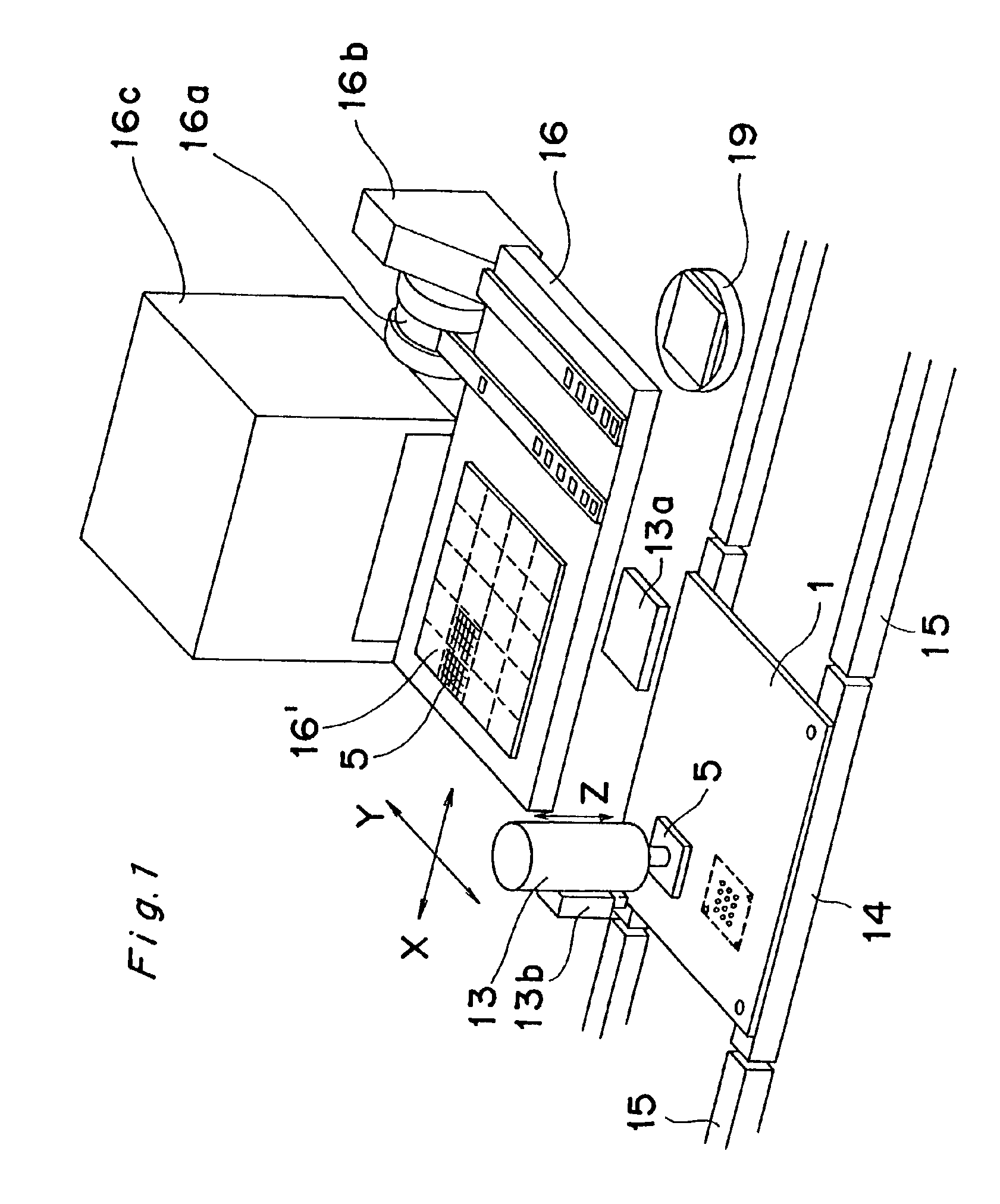
[0108]FIG. 1 is a perspective view showing an electronic component and the outline of a component mounting apparatus capable of implementing an electronic component mounting method, according to the first embodiment of the present invention. In this figure, the components that correspond to the constituent elements having substantially equivalent functions as the constituent elements shown in FIG. 14 and FIG. 16 which show the aforementioned prior art examples are denoted by the same reference numerals, and so forth in the figures described later. In FIG. 1, reference numerals denote respectively, 1 a printed board to be mounted with an electronic component, 13 a mounting head for holding an electronic component, 13a a component inspecting section for inspecting the posture and the like of the electronic component held by the mounting head, 13b a board recognizing section for recognizing a p...

second embodiment

[0137]Next, FIG. 5A shows an example of a pattern of BG connecting portions of a BGA component according to the present invention, while FIG. 5B is a view showing an example of parameter data of the arrangement of the BG connecting portions. In FIGS. 5A and 5B, reference numerals denote respectively, 5 a BGA component, 6 BG connecting portions (electrodes P11 through P44), 30 reference marks, 31 a recognition window, 35 arrangement parameter data, and 36 data bits.

[0138]The arrangement of the electrodes P11, P12 . . . , P44 of the pattern of the BG connecting portions 6 shown in FIG. 5A is translated into a model as shown in FIG. 5B in the form of the arrangement parameter data 35 of the BG connecting portions 6. According to this model, in the case of the example of the BG connecting portions 6 arranged in a matrix form shown in FIG. 5A, PLC is considered as the arrangement parameter data 35. In this case, PLC is the data expressing the presence or absence of the BG connecting port...

third embodiment

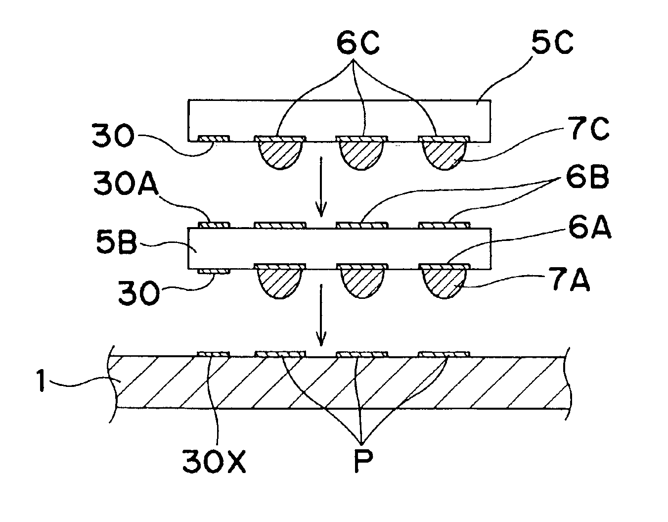
[0142]Next, FIG. 6A is a front view of reference marks provided on the surface opposite from the surface that has BG connecting portions of a BGA component according to the present invention, while FIG. 6B is a sectional view of the above.

[0143]In the third embodiment, the reference marks 30 are provided on the surface opposite from the surface that has the BG connecting portions 6, differently from the aforementioned first embodiment. The reference marks 30 are provided on the surface opposite from the surface on which the BG connecting portions 6 and the solder bumps 7 are provided. However, the BG connecting portions 6 and the reference marks 30 are simultaneously formed, and therefore, the relative positional relation is assured.

[0144]A mounting method of the BGA component 5 will be described. In the component take-out process (process S3) of the flowchart shown in FIG. 4, the component necessary for the mounting is supplied to and held in the component supplying section 16, whi...


PUM

PropertyMeasurementUnit
Timeaaaaaaaaaa
Lengthaaaaaaaaaa

Abstract

A component mounting method recognizes reference marks on a printed circuit board and an electronic component, and uses these reference marks to determine a shift between a position of the circuit board and a position of the electronic component. This shift is corrected and then the electronic component is mounted to the printed circuit board such that electrical connecting portions of the circuit board are connected to electrical connecting portions of the electronic component. The reference marks are formed simultaneously with corresponding electrical connecting portions via a mask, such that in order to accurately position the electrical connecting portions, it is only necessary to accurately relatively position the reference marks.

Description

[0001]This application is a Continuation-in-Part of application Ser. No. 09 / 319,779, filed Jun. 11, 1999 now U.S. Pat. No. 6,429,387.BACKGROUND OF THE INVENTION[0002]1. Technical Field[0003]The present invention relates to an electronic component having electrical connecting portions such as solder bumps or electrodes (lands, for example) exemplified by a solder bump component of a BGA (Ball Grid Array) type semiconductor component package (referred to as a BGA component hereinafter) represented by a CSP (Chip Size Package) or an electronic component such as QFP in forming an electronic circuit and relates to the mounting method and apparatus thereof.[0004]2. Description of Related Art[0005]In recent years, personal computers, portable telephones, information communications devices, multimedia electronic equipment, and the like have been compacted and provided with improved functions. Further, the electronic components and printed boards constituting electronic circuits have been ma...

Claims


Application Information

Patent Timeline
IPC IPC(8): H05K13/08H05K13/00H05K13/04H05K1/02H05K3/30
CPCH05K13/0465H05K13/08H05K1/0266H05K3/303Y10T29/49133Y10T29/53178Y10T29/53087Y10T29/4913Y10T29/49131Y10T29/49137Y10T29/53196H01L2224/81H05K13/0815
Inventor KURIBAYASHI, TAKESHINAKANO, KAZUYUKI
Owner PANASONIC CORP
Why Eureka
Try Eureka