Method of drilling holes with precision laser micromachining

a laser micromachining and laser micromachining technology, applied in the field of precision laser micromachining, can solve the problems of inability to move the holder with a level of accuracy, the current laser micromachining method, and the inability to drill features with the sub-micron accuracy and precision needed for photonic crystals

Inactive Publication Date: 2005-10-04
PANASONIC CORP
View PDF23 Cites 64 Cited by
  • Summary
  • Abstract
  • Description
  • Claims
  • Application Information

AI Technical Summary

Problems solved by technology

One reason that optical circuits have not been widely implemented is that there are manufacturing problems related to making photonic devices meet index of refraction specifications.
Current laser micromachining methods, such as direct writing, do not provide a way to drill features with the sub-micron accuracy and precision needed for photonic crystals.
The problem is that the holder cannot be moved with a level of accuracy suitable for manufacturing photonic crystals.
In addition to the spatial positioning errors, photonic structures may also suffer from blurring of the image of the laser beam as the feature sizes decrease to less than or equal to the size of the wavelength of the beam.

Method used


Image

  • Method of drilling holes with precision laser micromachining
  • Method of drilling holes with precision laser micromachining
  • Method of drilling holes with precision laser micromachining

Examples


second embodiment

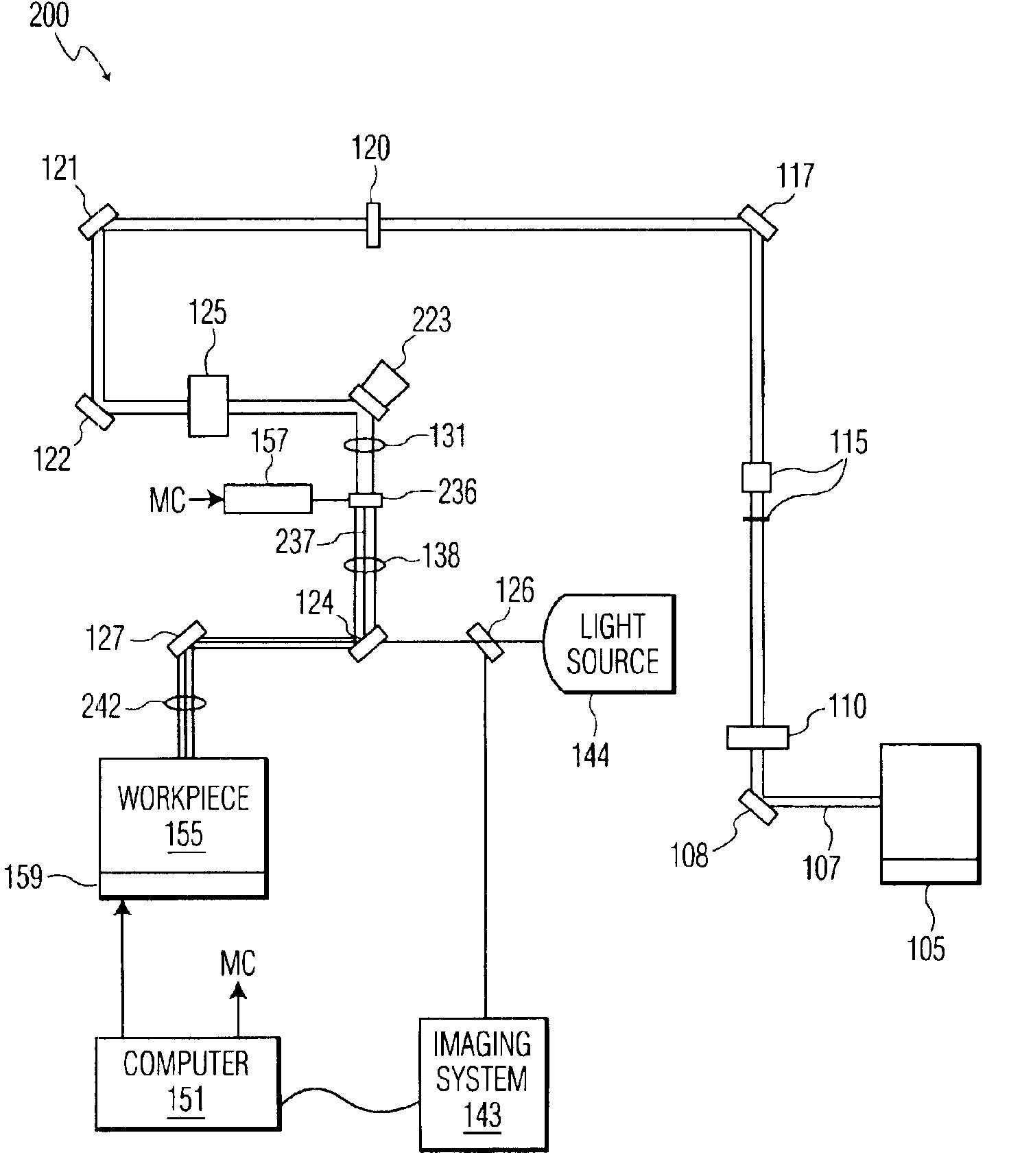
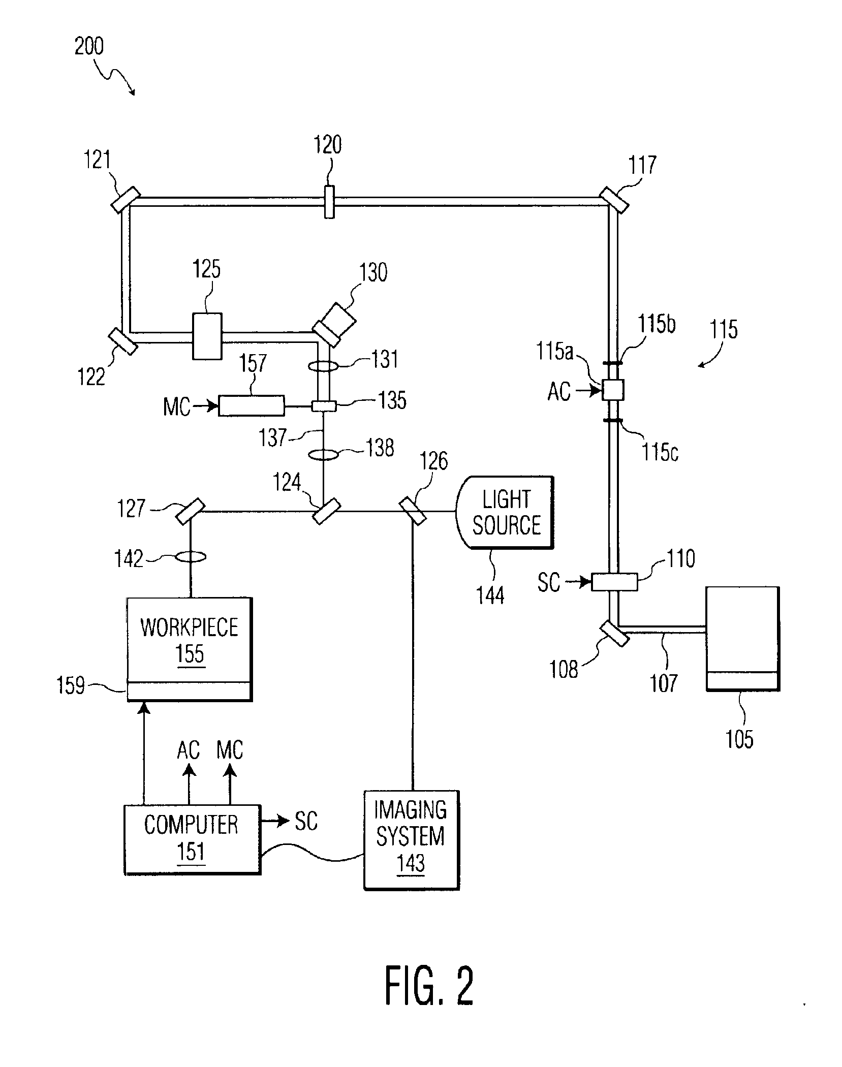
[0020]FIG. 2 is a block diagram of a drilling system 200. The system 100 includes a laser 105 which generates a laser beam 107 with a wavelength of 775 nm. In an alternative embodiment, the wavelength of laser beam 107 may be 387 nm. In such an alternative embodiment, the other characteristics of the system may be adjusted accordingly. Laser beam 107 travels along an optical path until it is incident upon first mirror 108. First mirror 108 is a conventional laser mirror having a high reflectivity at least at the wavelength of the laser beam 107. In this exemplary embodiment, first mirror 108 is highly reflective of 775 nm wavelength light. First mirror 108 redirects beam 107 along an optical path where it is incident upon shutter 110 which opens and closes to selectively illuminate work piece 155. Shutter 110 is a conventional laser shutter used to control the propagation of laser beam 107. In an exemplary embodiment, shutter 110 is an electric shutter controlled by a shutter contro...

first embodiment

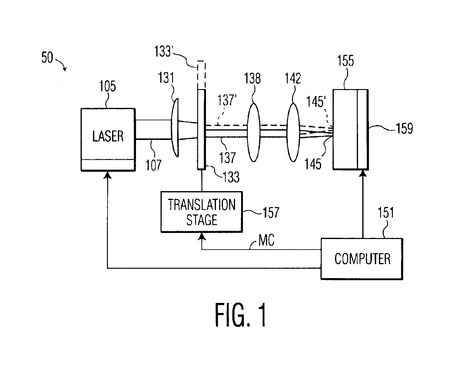
[0032]The combination of lens 138 and lens 142 provides the same function in this embodiment as the “eyepiece” lens 138 and the microscope objective lens 142 in the In an exemplary embodiment, 100× lens 142 has a 2 mm focal length and a 1 cm working distance. The exemplary embodiment may use an Ultra Long Working Distance Lens (ULWD) having a working distance of 1 cm as the lens 142. Alternatively, a conventional 2 mm lens may be used along with an air knife to remove any material that is ablated from the work piece.

[0033]The combination of lens 138 (focal length f1=60 mm) and 100× lens 142 (focal length f2=2 mm) creates a de-magnification of thirty (f1 / f2) of sub-beam 137 upon work piece 155. Thus, the size of the image of the mask 135 on the work piece is 1 / 30th the size of the image at the mask 135. This de-magnification of thirty means a reduced-size image of sub-beam 137 is moved one-thirtieth of the distance that aperture 135 is moved. In one example, therefore, when aperture...


PUM

PropertyMeasurementUnit
sizeaaaaaaaaaa
sizeaaaaaaaaaa
wavelengthaaaaaaaaaa

Abstract

The invention is an apparatus and a method for drilling holes in a work piece with a laser. A laser beam is received by the optical system and directed along an optical path. The system directs the laser beam through a moveable mask aperture creating a sub-beam, that is reduced in size by a lens system as it is imaged onto a work piece. Multiple features are formed in the work piece by moving the mask.

Description

CROSS REFERENCE TO RELATED APPLICATION[0001]This application claims the benefit under Title 35 U.S.C. § 119(e) of U.S. Provisional Application No. 60 / 375,741 filed on Apr. 26, 2002, the contents of which are incorporated herein by reference.FIELD OF THE INVENTION[0002]The present invention relates to precision laser micromachining. More specifically, it relates to a method of and a system for laser micromachining to obtain precise alignment of drilling laser beams and for fabricating products, having sub-micron features, with precision and accuracy. One embodiment may be used to fabricate photonic devices such as photonic crystals.BACKGROUND OF THE INVENTION[0003]Photonic devices and microphotonics provide exciting potential for furthering the advancement of technology historically served by microelectronics. Photonic devices may be used as frequency selection filters to enable large volumes of data to travel along optical fibers and to be routed to their final destinations. As ligh...

Claims


Application Information

Patent Timeline
Patent Type & Authority Patents(United States)
IPC IPC(8): B23K26/00B23K26/06B23K26/38B23K26/04
CPCB23K26/04B23K26/0656B23K26/381B23K26/043B23K26/4075B23K26/382B23K26/066B23K26/40B23K2103/50
Inventor LI, MINGISHIZUKA, MAKOTOLIU, XINBING
Owner PANASONIC CORP
Why Eureka
Try Eureka