

Electrically isolated pillars in active devices
- Summary
- Abstract
- Description
- Claims
- Application Information
AI Technical Summary
Benefits of technology
Problems solved by technology
Method used
Image

Examples
Example
DETAILED DESCRIPTION OF THE DRAWINGS
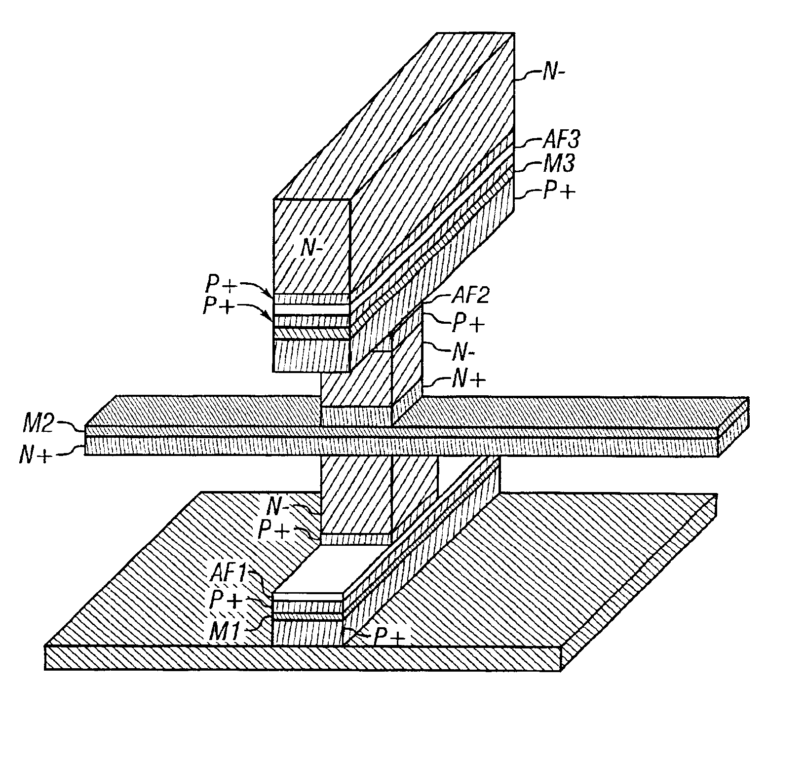
[0029]According to a first aspect of the invention, at least one portion of an active device is made by performing sequential patterning steps in a “back-to-back” fashion, i.e, without the interposition of a dielectric fill step between the patterning steps. Note that other processing steps can be carried out, such as but not limited to sidewall oxidations, sidewall cleaning operations such as solvent dips, and anneals (such as furnace anneals or RTAs) without changing the “back-to-back” nature of the process described herein.
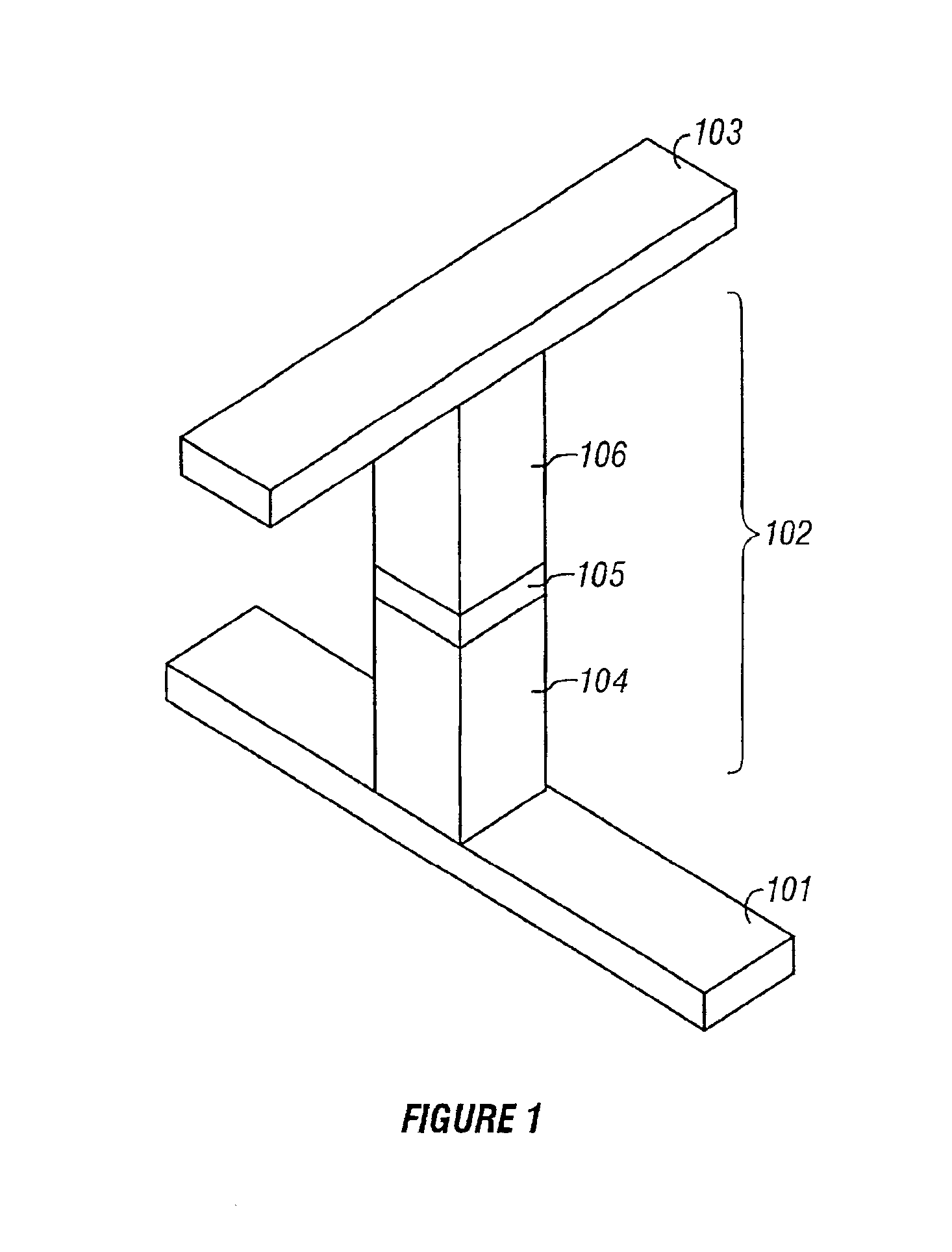
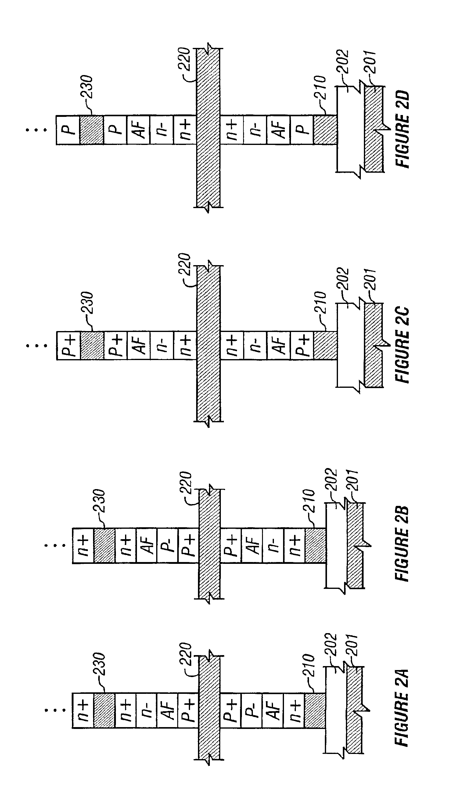
[0030]In one embodiment, a first patterning operation includes etching a plurality of layers into a plurality of strips, thereby forming rails oriented in a first direction. A second patterning operation includes etching at least one strip of the first plurality of strips in a second direction, wherein the second direction is typically orthogonal to the first direction. The first and second etches form pillars, which include ...
PUM
 Abstract
Description
Claims
Application Information