
System and Method for Modifying a Test Pattern to Control Power Supply Noise

Inactive Publication Date: 2008-04-03
IBM CORP
View PDF5 Cites 23 Cited by
  • Summary
  • Abstract
  • Description
  • Claims
  • Application Information

AI Technical Summary

Benefits of technology

[0011]The illustrative embodiments provide a system and method for modifying test patterns to control power supply noise for more accurate determination of the minimum functional voltage (Vminf) of an integrated circuit device. With the system and method, a portion of a sequence of states in a test sequence of a test pattern is modified so as to achieve a circuit voltage, e.g., an on-chip voltage, which approximates the circuit voltages produced by the application of other portions of the sequence of states in the same or different test sequences. Alternatively, an expected circuit voltage during actual operating conditions may be determined and used as a basis for modifying the test sequence of a test pattern so as to achieve a circuit voltage using the test sequence that approximates the expected circuit voltage during actual operating conditions. In this way, false failures due to noise in the voltage supply may be removed from the testing as a source of failures. As a result, a more accurate determination of the minimum functional voltage (Vminf) is obtained.
[0012]In one illustrative embodiment, the modification to the test sequence is performed by inserting (or removing) one or more hold state cycles into the test sequence prior to test state cycles so as to modify the sequence of current draws prior to testing of the functional logic. This insertion (or removal) of hold state cycles helps to cancel out affects on on-chip voltage (Vdd) during test cycles by current draws during test setup cycles.
[0014]The insertion (or removal) of hold state cycles does not change the actual testing of the functional logic of the integrated circuit device, but instead only alters the voltage response of the functional logic. The insertion (or removal) of the one or more hold state cycles allows the on-chip voltage to recover or rebound before additional current draws are required by the subsequent test state. As a result, the cumulative affect of current draws by the various states in the test sequence is lessened and on-chip voltage droops are minimized.
[0015]In an alternative illustrative embodiment, one or more scan-shift state cycles may be inserted (or removed) into the test sequence rather than, or in addition to, inserting (or removing) hold state cycles. The scan-shift state cycles may be inserted (or removed) such that the on-chip voltage (Vdd) response to the current demand of the scan-shift state cycles partially cancels that of the test state cycles, thereby reducing the on-chip voltage (Vdd) droop.
[0017]With either approach, the voltage waveform response of the integrated circuit device to prior state cycles of the test sequence, or a different test sequence, may be used to determine whether one or more hold state cycles and / or scan-shift state cycles should be inserted (or removed) prior to present test state cycles in the test sequence. Essentially, the goal is to obtain as much as possible a consistent voltage response across multiple test state cycles of the same or different test sequence so as to minimize voltage droops that may give rise to false failures during testing. The insertion of each hold state cycle provides additional time between test states so as to provide the on-chip voltage with time to rebound. The removal of hold state cycles shifts the test state cycles so as to be closer to being coincident with a maximum or peak rebound of the on-chip voltage (Vdd) response to prior state cycle current draws. The insertion (or removal) of each scan-shift state cycle provides a partial cancellation of the on-chip voltage (Vdd) response of subsequent test state cycles and helps to eliminate the affects of prior test setup cycles on the on-chip voltage (Vdd) response.
[0018]In one illustrative embodiment, a method is provided for testing an integrated circuit device. The method may comprise determining a voltage response of the integrated circuit device to a test state sequence and modifying a test pattern waveform based on the determined voltage response so as to reduce noise in the voltage response during the test state sequence. The method may further comprise applying the modified test pattern waveform to the integrated circuit device and determining a minimum functional voltage for the integrated circuit device based on the application of the modified test pattern waveform.

Problems solved by technology

A problem arises, however, when using LBIST to determine Vminf in that the integrated circuit device does not operate in an idealized manner in which the voltage inside the integrated circuit device, i.e. the on-chip voltage Vdd, is at a constant voltage at all times. To the contrary, the on-chip voltage Vdd is a complex function involving characteristics of the power supply (e.g., resistance, capacitance, inductance at the chip, package, and board levels, etc.) and the current-vs-voltage characteristics of the circuits on the chip, i.e. in the integrated circuit device.
Short term current demand which is less than average will result in increased charge stored in the on-chip capacitance.
Thus, as the states of the LBIST change, the voltage in the on-chip capacitance changes thereby possibly causing droops in the on-chip voltage Vdd.
Such changes in the on-chip voltage Vdd from an idealized constant voltage is referred to as power supply noise.
If the on-chip voltage Vdd droops too far, i.e. the power supply noise is too great, the corresponding test may fail.
Thus, depending upon the sequence of states used for the particular tests, certain tests may fail at different external voltages from the voltage supply.
Thus, there is an uncertainty in the determination of the Vminf calculated using such LBIST in the known technology.
In this way, false failures due to noise in the voltage supply may be removed from the testing as a source of failures.

Method used


Image

  • System and Method for Modifying a Test Pattern to Control Power Supply Noise
  • System and Method for Modifying a Test Pattern to Control Power Supply Noise
  • System and Method for Modifying a Test Pattern to Control Power Supply Noise

Examples


Embodiment Construction

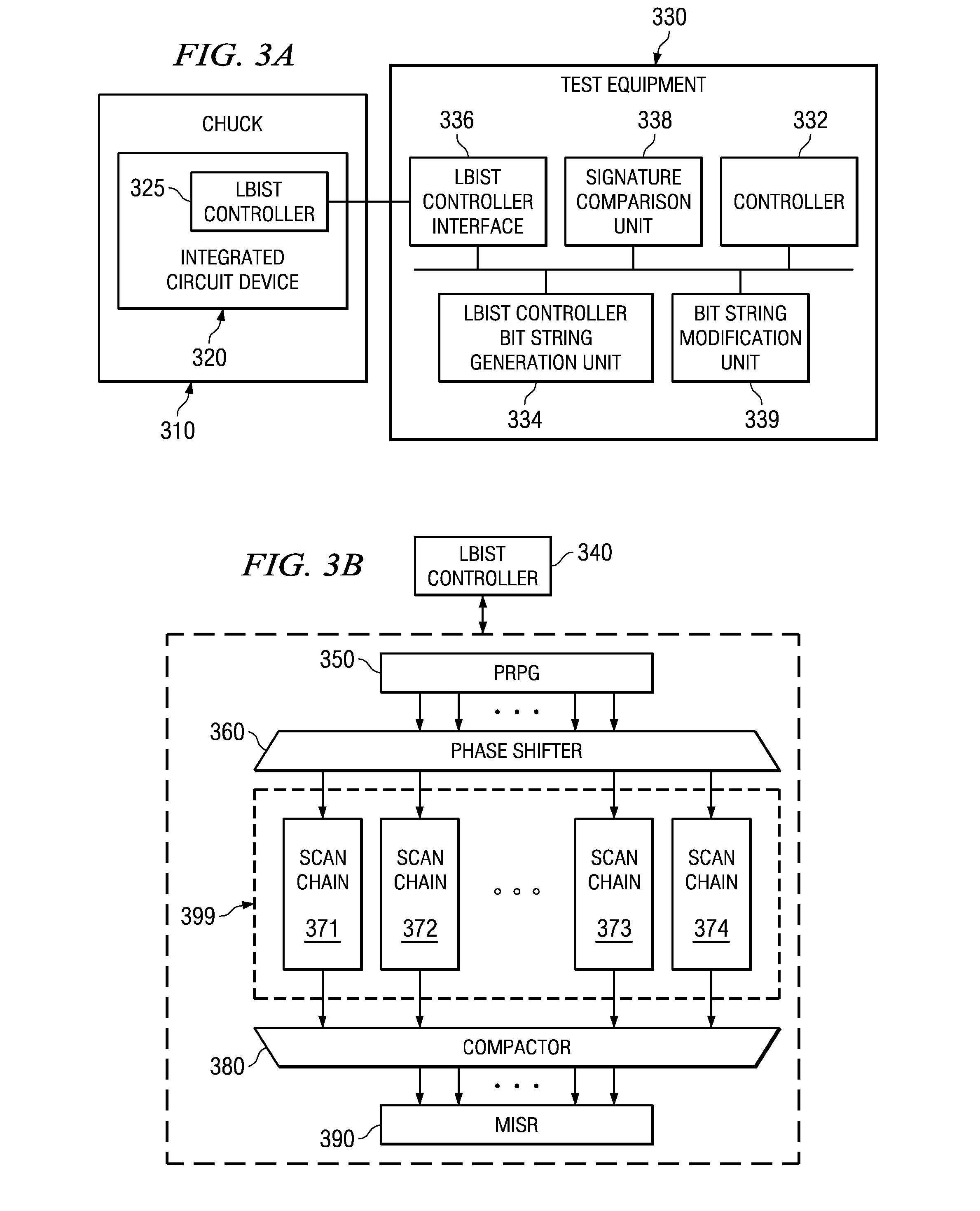
[0037]The illustrative embodiments provide a mechanism by which test patterns may be modified to control power supply noise for more accurate determination of the minimum functional voltage (Vminf) of an integrated circuit device, such as an integrated circuit chip, for example. The mechanism of the illustrative embodiments may be implemented in a single computing device or may be distributed across a plurality of computing devices in communication with one another via one or more data networks. For example, a client computing device may communicate with a server computing device, via one or more data networks, in order to provide the server computing device with an model of an integrated circuit device that may be simulated and tested in accordance with the illustrative embodiments of the present invention as set forth hereafter.

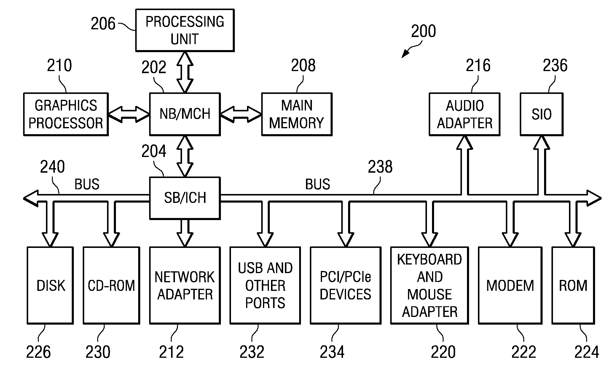
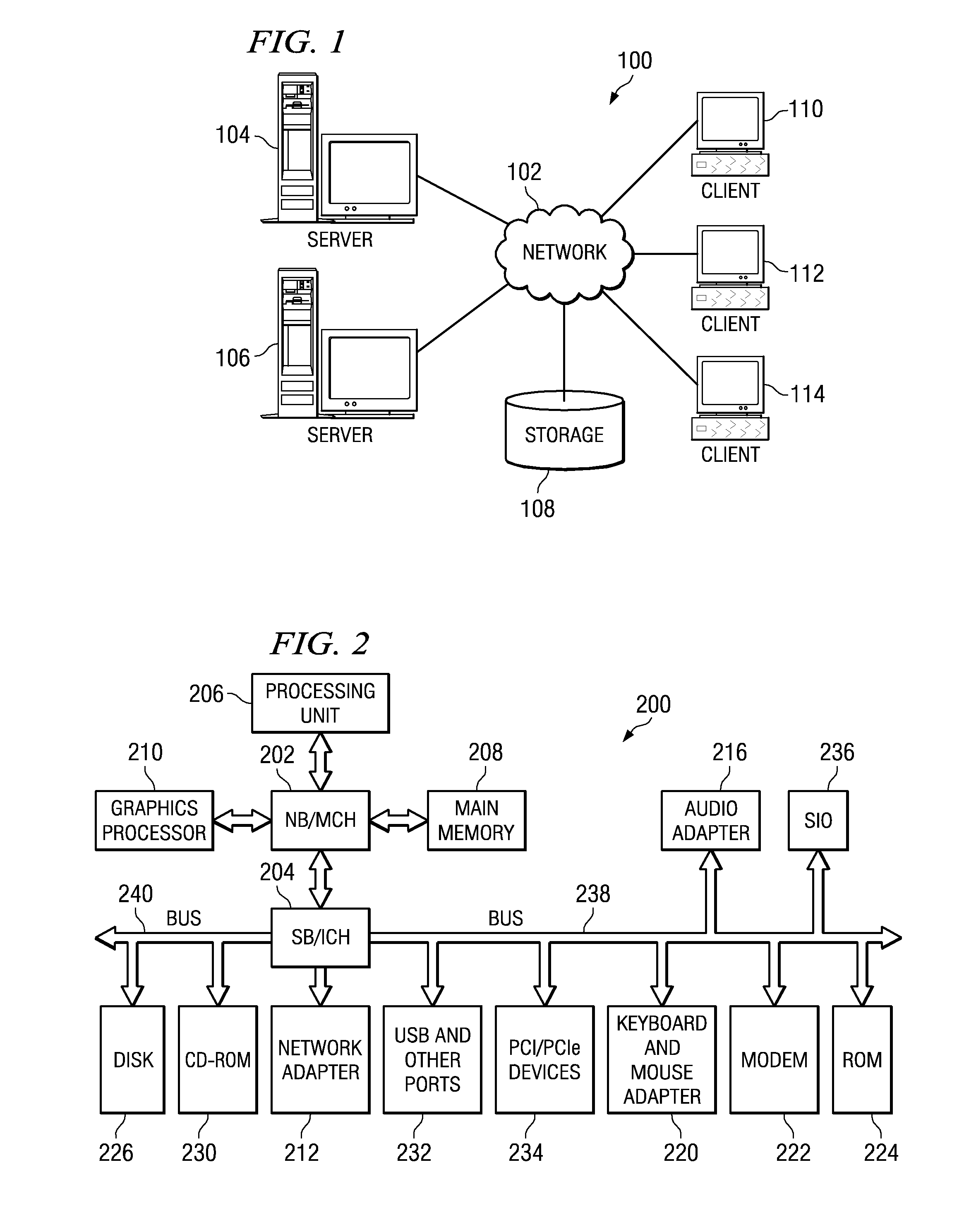
[0038]With reference now to the figures and in particular with reference to FIGS. 1-2, exemplary diagrams of data processing environments are provided in w...


PUM


Abstract

A system and method for modifying a test pattern to control power supply noise are provided. A portion of a sequence of states in a test sequence of a test pattern waveform is modified so as to achieve a circuit voltage, e.g., an on-chip voltage, which approximates a nominal circuit voltage, such as produced by the application of other portions of the sequence of states in the same or different test sequences. For example, hold state cycles or shift-scan state cycles may be inserted or removed prior to test state cycles in the test pattern waveform. The insertion / removal shifts the occurrence of the test state cycles within the test pattern waveform so as to adjust the voltage response of the test state cycles so that they more closely approximate a nominal voltage response. In this way, false failures due to noise in the voltage supply may be eliminated.

Description

BACKGROUND[0001]1. Technical Field[0002]The present application relates generally to an improved data processing system and method. More specifically, the present application is directed to a system and method for modifying a test pattern so as to control power supply noise during testing of an integrated circuit device. In particular, the system and method of the illustrative embodiments set forth hereafter are directed to controlling power supply noise during testing so as to provide a more accurate determination of a minimum functional voltage of an integrated circuit device when compared to known techniques.[0003]2. Description of Related Art[0004]Testing of integrated circuit devices is an important factor in ensuring proper functionality of the integrated circuit devices as well as for determining the functional capabilities of the integrated circuit devices for categorization purposes, e.g., binning. As integrated circuit devices have become more complex, in an effort to redu...

Claims


Application Information

Patent Timeline
IPC IPC(8): G01R31/28G06F11/00
CPCG01R31/318575G01R31/318536
Inventor DHONG, SANG H.FLACHS, BRIANGERVAIS, GILLESMICHAEL, BRAD W.RILEY, MACK W.
Owner IBM CORP
Learn More