Semiconductor integrated circuit device and wiring arranging method thereof

a technology of integrated circuit device and integrated circuit, which is applied in the direction of semiconductor device, semiconductor/solid-state device details, electrical apparatus, etc., can solve the problems of high manufacturing cost and delay in signal transmission

Inactive Publication Date: 2005-11-08
KK TOSHIBA
View PDF14 Cites 5 Cited by
  • Summary
  • Abstract
  • Description
  • Claims
  • Application Information

AI Technical Summary

Benefits of technology

[0017]As described above, the present invention provides a semiconductor integrated circuit device and a wiring arranging method, which make it possible to achieve connection of an optional I / O slot without changing the wiring pattern within the chip.

Problems solved by technology

If the wiring is long like the wiring 17, problems such as delay of the signal transmission are generated.
However, the chip must be redesigned for changing the position of the I / O slot, leading to a high manufacturing cost.

Method used


Image

  • Semiconductor integrated circuit device and wiring arranging method thereof
  • Semiconductor integrated circuit device and wiring arranging method thereof
  • Semiconductor integrated circuit device and wiring arranging method thereof

Examples


Embodiment Construction

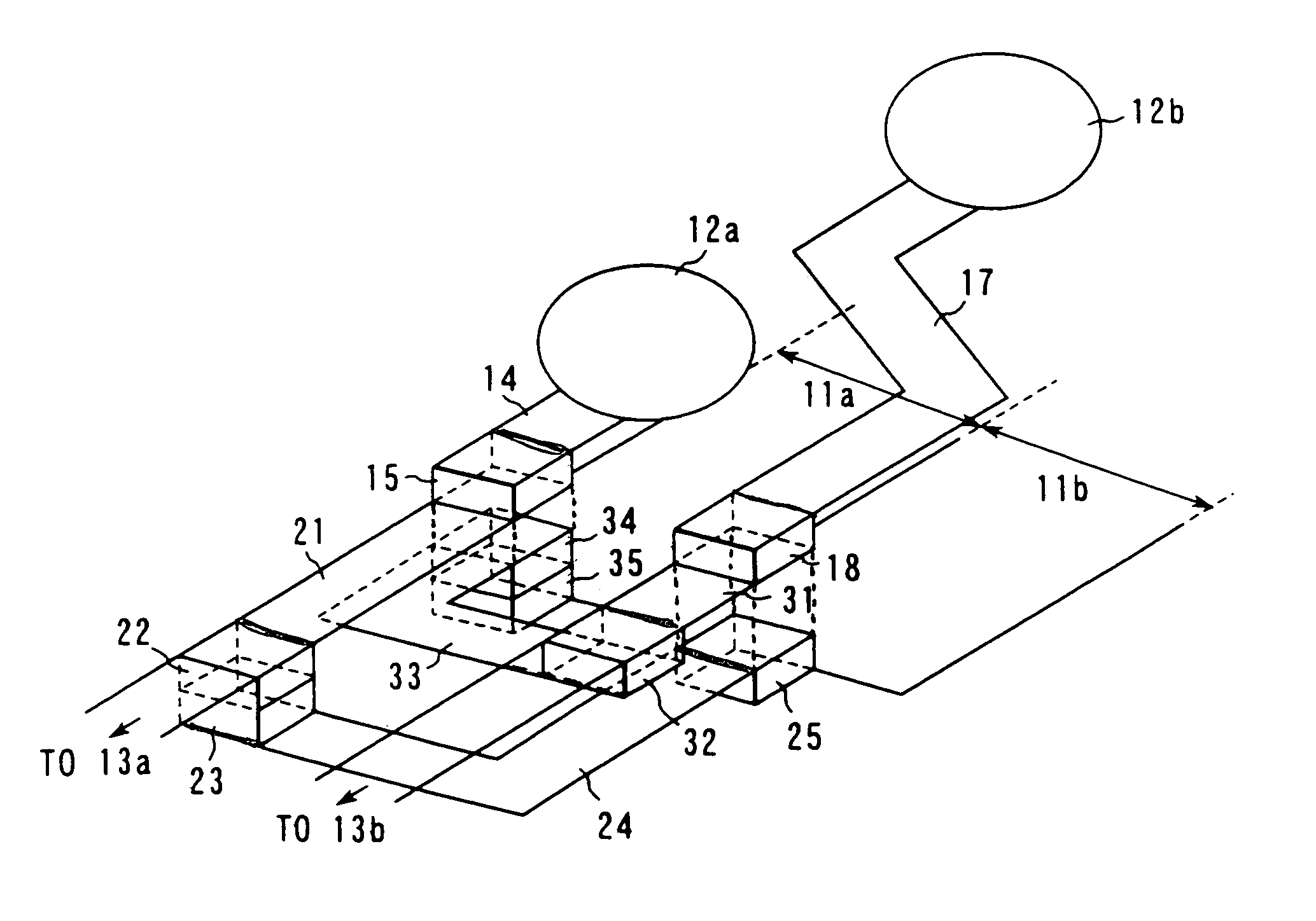
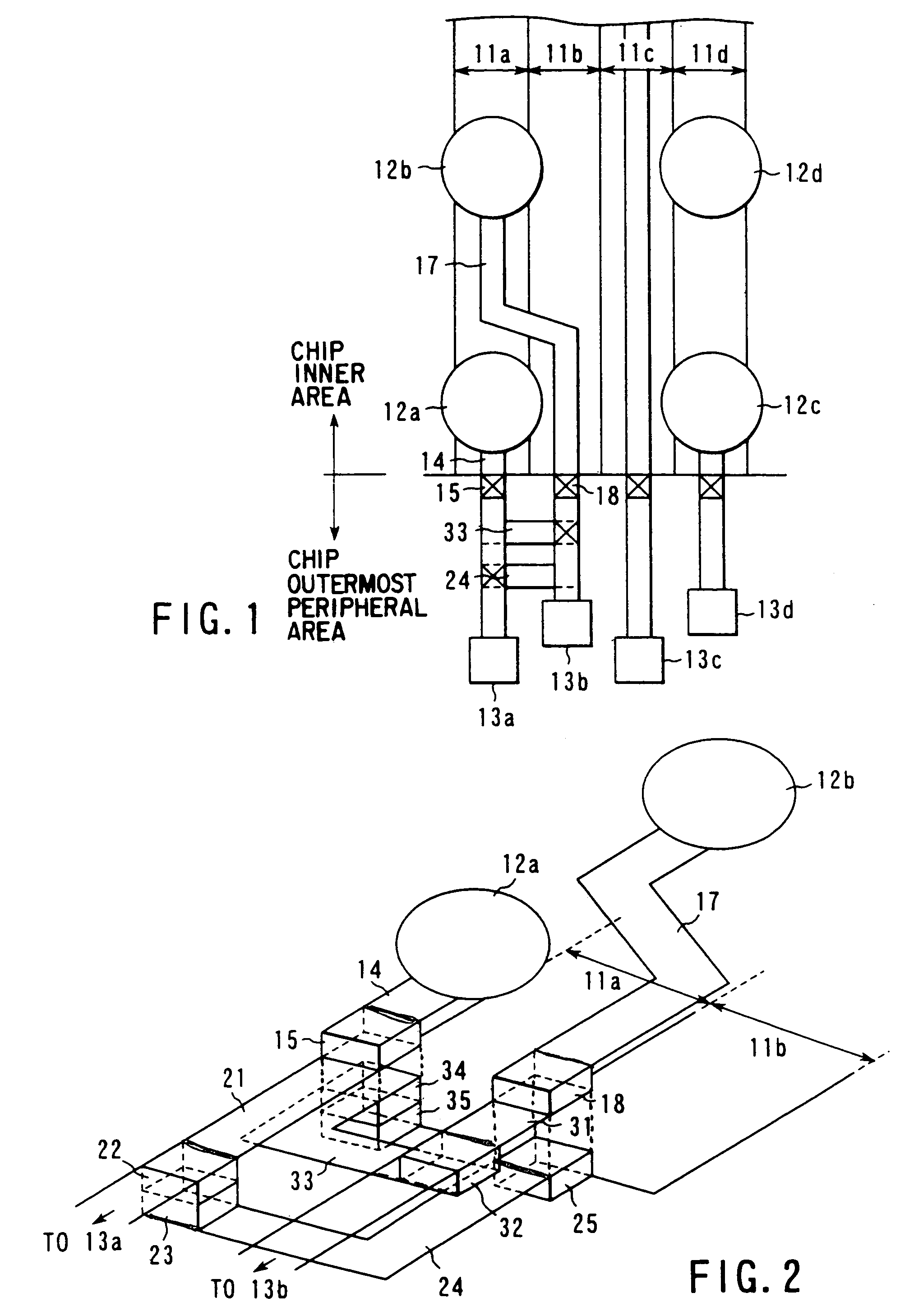
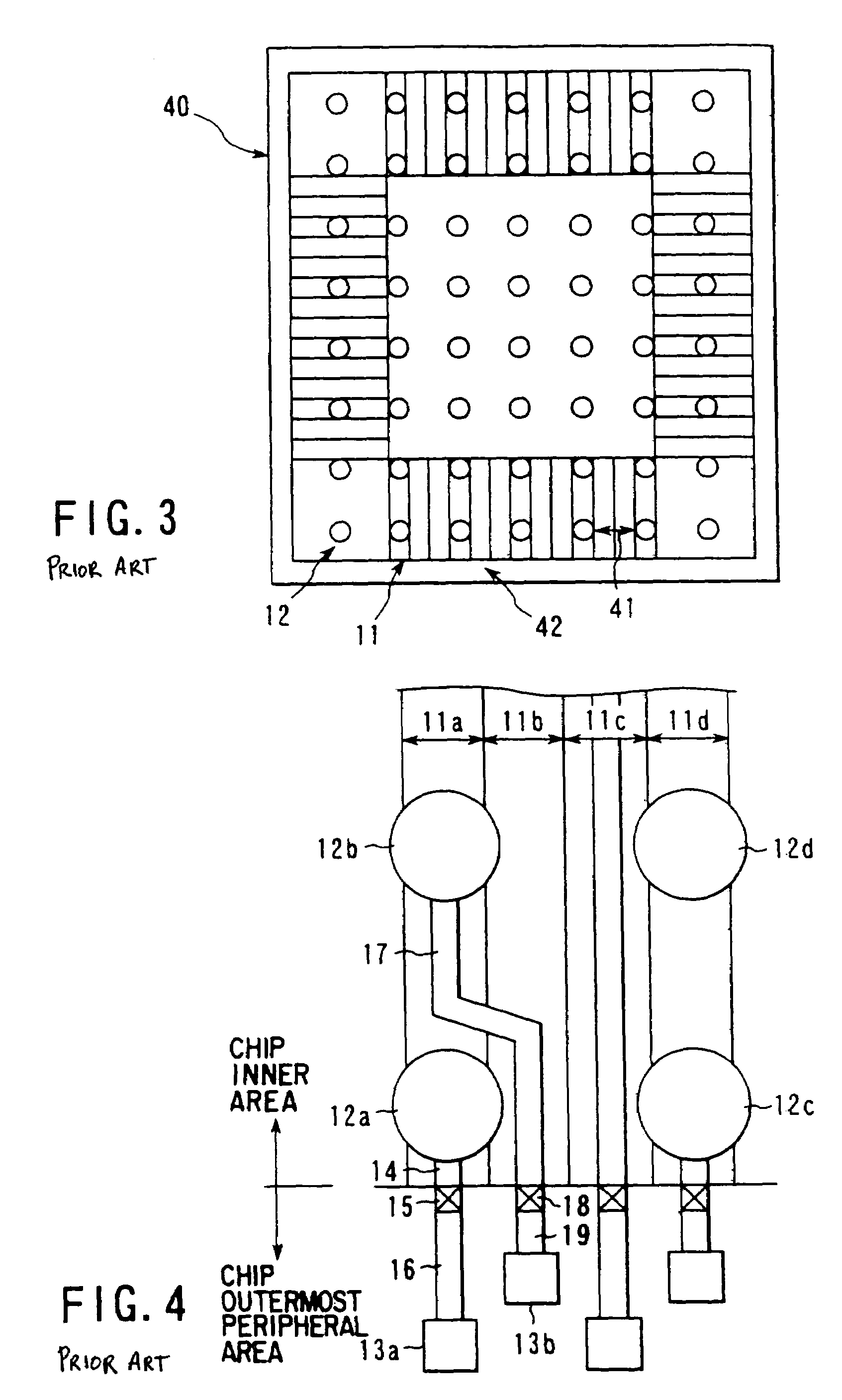
[0024]A semiconductor integrated circuit device of the present invention will now be described with reference to the accompanying drawings. As shown in FIG. 1, specifically, I / O slots 11a, 11b, 11c and 11d are arranged in the chip inner area. Pads 12a, 12b are arranged above the I / O slot 11a among these I / O slots 11a to 11d. Also, pads 12c, 12d are arranged above the I / O slot 11d. The pad 12a is connected by the wiring 14 to the via 15 formed in the chip outermost peripheral area. Likewise, the pad 12b is connected by the wiring 17 to the via 18 formed in the outermost peripheral area. These wirings 14, 17 constitute the standard pattern of the uppermost layer of the chip inner area. Further, defect analyzing pads 13a, 13b, 13c, 13d are arranged in the chip outermost peripheral area.

[0025]In this embodiment, the pads 12a and 12b can be connected to the I / O slots 11b and 11a, respectively, by using rewiring 24, 33 formed in the chip outermost peripheral area. The connection of the pa...


PUM


Abstract

Even where an I / O cell requiring good characteristics is alloted to an I / O slot corresponding to the uppermost standard pattern wiring, a pad can be connected to the I / O slot by forming rewiring in the chip outermost peripheral area.

Description

CROSS-REFERENCE TO RELATED APPLICATION[0001]This is a division of application Ser. No. 10 / 081,109, filed Feb. 25, 2002 now U.S. Pat. 6,844,630 (allowed), which is a continuation of application Ser. No. 09 / 527,563, filed Mar. 16, 2000 (abandoned), and claims priority of Japanese Patent Application No. 11-069907, filed Mar. 16, 1999, all of which are incorporated herein by reference.BACKGROUND OF THE INVENTION[0002]The present invention relates to a semiconductor integrated circuit device make use of an area pad and a wiring arranging method thereof.[0003]A signal between a chip of a semiconductor integrated circuit and a package is inputted / outputted through a wiring arranged in an I / O slot of the chip and a wiring between input / output pads. An I / O cell, e.g., input / output buffer, is connected to the I / O slot. Each of the I / O slot and the wiring arranged in the I / O slot is called I / O slot herein later.[0004]As shown in FIG. 3, an I / O slot 11 is arranged in a periphery of a chip 40, a...

Claims


Application Information

Patent Timeline
Patent Type & Authority Patents(United States)
IPC IPC(8): H01L23/48H01L23/50H01L21/82H01L21/00
CPCH01L23/50H01L2924/15173H01L2924/0002H01L2924/00H01L27/0207H01L27/04
Inventor SAKAMOTO, SHINSUKEINBE, YASUOYAGINUMA, MASAKAZUHORIKAWA, KAZUNARISEI, TOSHIKAZU
Owner KK TOSHIBA
Why Eureka
Try Eureka