Display device and drive method for driving the same

a display device and drive method technology, applied in the field of active matrix display devices, can solve problems such as more complicated device configuration, and achieve the effects of reducing potential drops, prolonging the life of the device, and increasing pitch

Active Publication Date: 2013-11-19
SHARP KK
View PDF18 Cites 0 Cited by
  • Summary
  • Abstract
  • Description
  • Claims
  • Application Information

AI Technical Summary

Benefits of technology

[0040]According to the first aspect of the present invention, at least one of the switch elements in the same group on the display control circuit is controlled to be on during a period required for providing a corresponding image signal to a corresponding video signal line, and a time point at which a part of the switch elements in the same group is turned off is controlled to vary from a time point at which the remaining switch elements are turned off, thereby making it possible to achieve display devices employing, for example, the dot-sequence driving system, the video signal line time-division driving system, the phase expansion driving system, etc., which allow either suppression of potential drops on video signal lines due to fieldthrough phenomenon, which is a problem caused by turning on / off transistors used in switch elements coupled to the video signal lines, or extension of short device life, which is a problem caused by turning on / off the transistors.
[0041]According to the second aspect of the present invention, by employing the video signal line time-division driving system, it becomes possible to increase the pitch between connections of output terminals to video signal lines in display devices, and it also becomes possible to either suppress potential drops on video signal lines due to fieldthrough phenomenon, which is a problem caused by turning on / off transistors used in switch elements coupled to the video signal lines, or extend short device life, which is a problem caused by turning on / off the transistors.
[0042]According to the third aspect of the present invention, it is possible to achieve color display devices with video signal lines being divided into groups, each consisting of three adjacent video signal lines respectively coupled to three varieties of pixel formation portions for displaying three predetermined primary colors, which allow either suppression of potential drops on video signal lines due to fieldthrough phenomenon, which is a problem caused by turning on / off transistors used in switch elements coupled to the video signal lines, or extension of short device life, which is a problem caused by turning on / off the transistors.
[0043]According to the fourth aspect of the present invention, since the switch elements are thin-film transistors each having a semiconductor layer made of microcrystalline silicon, amorphous silicon or an oxide semiconductor, it is possible to sufficiently suppress the impact of fieldthrough phenomenon, which tends to increase especially due to parasitic capacitance of the elements becoming comparatively high to achieve a sufficient drive rate, and it is also possible to sufficiently extend device life, which tends to be short because the threshold voltage shift occurs relatively easily.
[0044]According to the fifth aspect of the present invention, the display control circuit controls the switch elements such that, for each horizontal scanning period, the switch elements in the same group are turned on at approximately the same time, with a part of the group being the last to be turned off, so that only the parasitic capacitance of the last switch element to be turned off has impact, and therefore it is possible to suppress potential drops on video signal lines due to fieldthrough phenomenon.
[0045]According to the sixth aspect of the present invention, since the switch elements are thin-film transistors each having a semiconductor layer and the last part to be turned off among the switch elements in the same group is smaller than the remaining switch elements, it is possible to further reduce the parasitic capacitance of the last switch element to be turned off, thereby further suppressing potential drops on video signal lines due to fieldthrough phenomenon.

Problems solved by technology

Therefore, in some cases, a so-called phase expansion driving system (phase expansion processing system) is employed to extend the sampling time and the charging time, which, however, results in a more complicated device configuration when compared to the dot-sequence driving system.

Method used


Image

  • Display device and drive method for driving the same
  • Display device and drive method for driving the same
  • Display device and drive method for driving the same

Examples


first embodiment

[0061]

[0062]

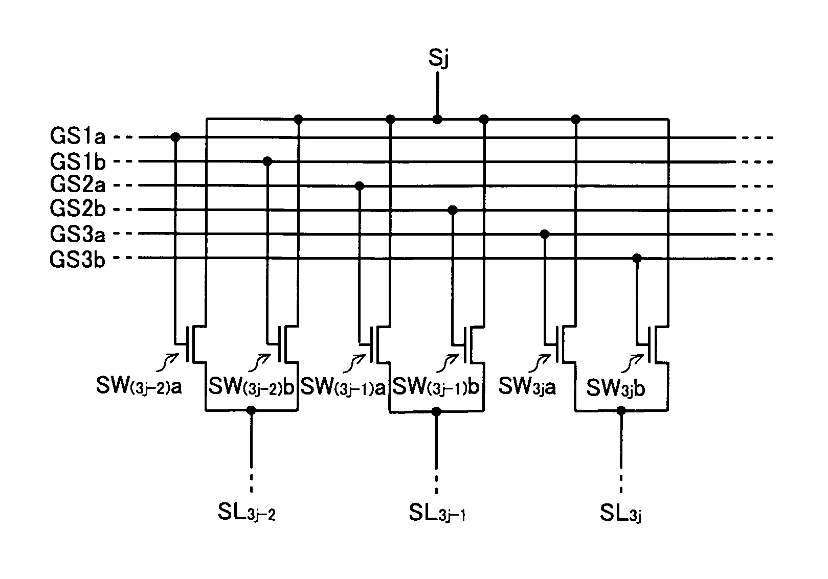
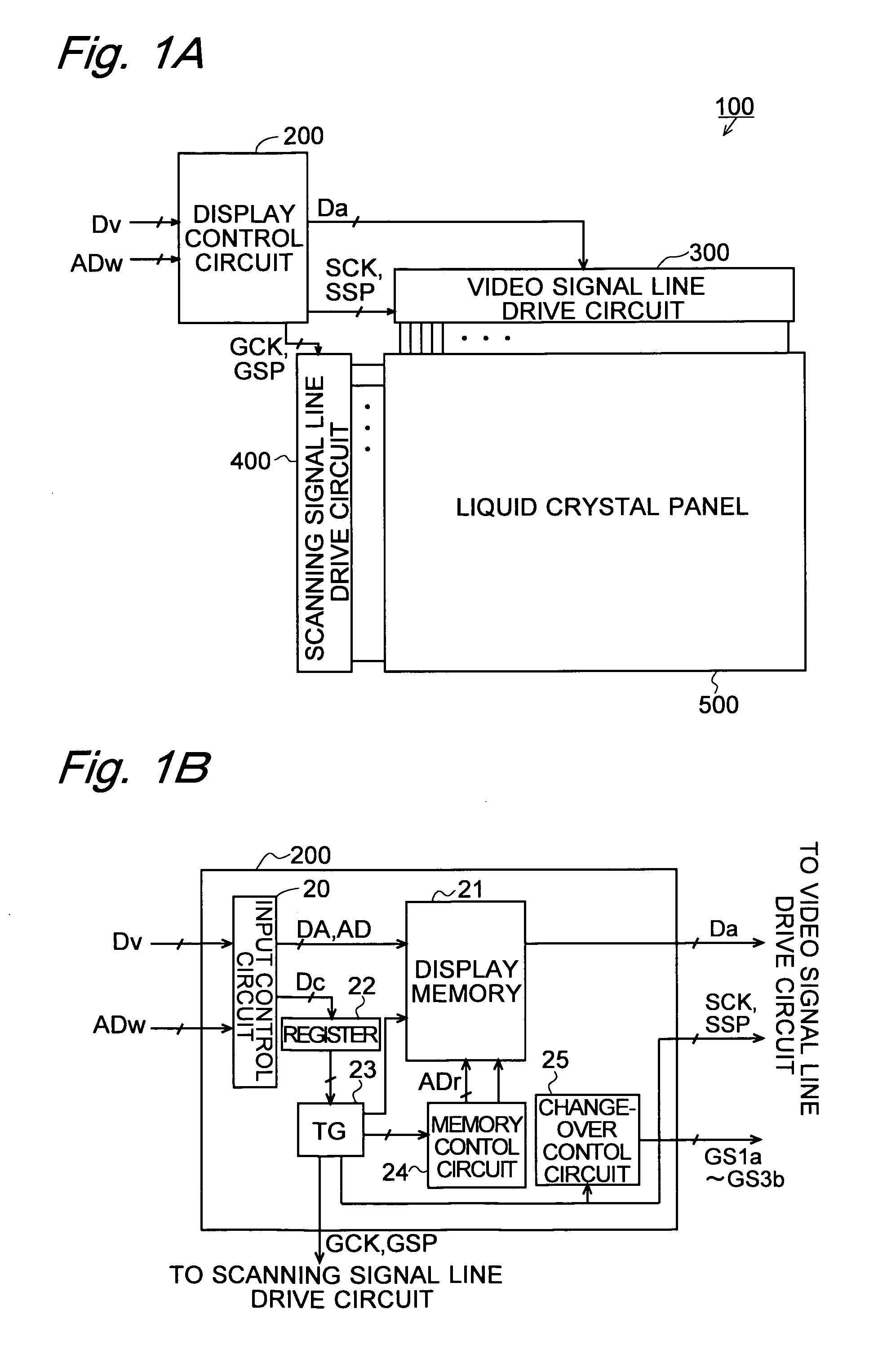
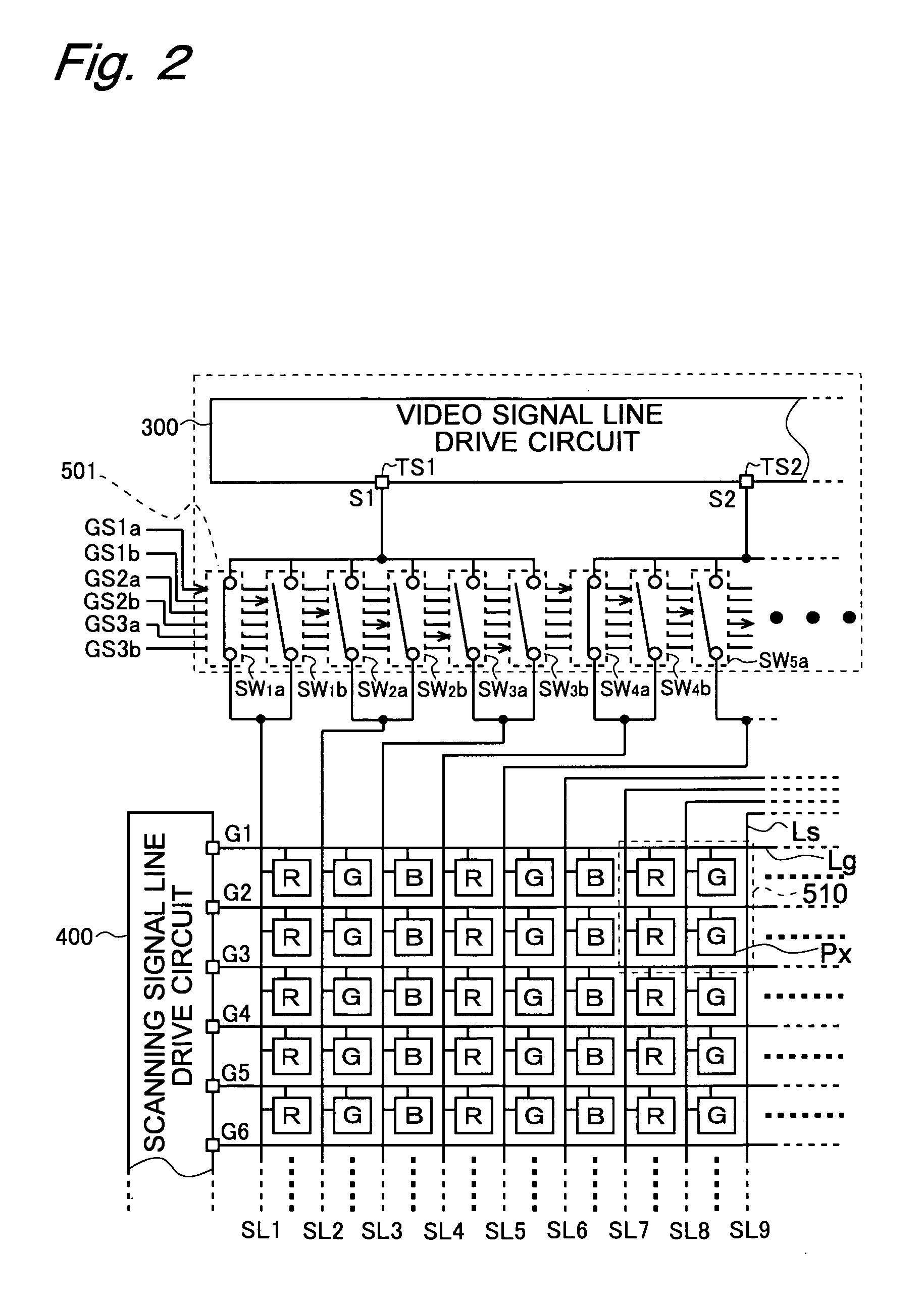
[0063]FIG. 1A is a block diagram illustrating the configuration of a liquid crystal display device according to a first embodiment of the present invention. This liquid crystal display device 100 includes a display control circuit 200, a video signal line drive circuit (also referred to as a “column electrode drive circuit” or a “source driver”) 300, a scanning signal line drive circuit (also referred to as a “row electrode drive circuit” or a “gate driver”) 400, and an active-matrix liquid crystal panel 500.

[0064]As a display portion of the liquid crystal display device 100, the liquid crystal panel 500 includes a plurality of scanning signal lines (row electrodes) corresponding to horizontal scanning lines in an image represented by image data Dv received from a CPU or suchlike in an external computer, a plurality of video signal lines (column electrodes) crossing the scanning signal lines, and a plurality of pixel formation portions provided at their corresponding int...

second embodiment

[0106]

[0107]

[0108]A liquid crystal display device 100 according to a second embodiment of the present invention is configured in approximately the same manner as in the first embodiment, except for the configuration and operation of switch elements SWi of a liquid crystal panel, and the same elements are denoted by the same characters with any detailed descriptions thereof omitted.

[0109]Also, unlike in the first embodiment, TFTs functioning as the switch elements SWi are formed in the same size (concretely, channel width) as in conventional configurations, rather than in smaller size than conventional for the purpose of reducing parasitic capacitance Cgd. Therefore, each one of them alone has sufficient driving performance of driving the video signal line, but cannot suppress fieldthrough phenomenon by itself. In the present embodiment, however, the switch elements SWi operate to allow extension of short device life, which is another of their problems. Hereinafter, the operation of ...

third embodiment

[0118]

[0119]

[0120]A liquid crystal display device 100 according to a third embodiment of the present invention is configured in the same manner as in the second embodiment, except for the operation of switch elements SWi of a liquid crystal panel, and the same elements are denoted by the same characters with any detailed descriptions thereof omitted. Note that TFTs functioning as the switch elements SWi are also configured in the same manner as in the second embodiment.

[0121]However, in the present embodiment, the operation is performed so as to allow further extension of a short device life of the switch elements SWi compared to the second embodiment. Hereinafter, the operation of the switch elements SWi will be described with reference to FIG. 7, along with a method for driving the liquid crystal panel.

[0122]

[0123]FIG. 7 is a timing chart describing a drive method for the instant liquid crystal display device. For various signals, other than changeover control signals GS1a to GS3b...


PUM


Abstract

A display device of at least one embodiment of the present invention has a connection changeover circuit, including switch elements for time-division driving, formed on a liquid crystal panel, and the switch elements are paired so that two switch elements in each pair are connected in parallel to one video signal line. The paired switch elements are turned on at the same time, and immediately before one of the switch elements is turned off upon completion of a charging period for its corresponding video signal line, only the other switch element is turned off. As a result, while maintaining drive performance, it is possible to solve the impact of fieldthrough phenomenon caused by one of the switch elements, which are transistors, and also reduce parasitic capacitance formed in the other switch element, thereby suppress the impact of fieldthrough phenomenon caused by that switch element.

Description

TECHNICAL FIELD[0001]The present invention relates to active-matrix display devices, more specifically to a display device which employs, for example, a dot-sequence driving system, a phase expansion driving system or a video signal line time-division driving system, and a drive method therefor, in which video signals are sequentially outputted from a drive circuit through switch elements to a number of video signal lines for transmitting the video signals to a plurality of pixel formation portions for forming an image to be displayed.BACKGROUND ART[0002]In general, an active-matrix liquid crystal display device has a liquid crystal panel, including two substrates with a liquid crystal layer provided therebetween, as a display portion, in which a plurality of data lines as video signal lines and a plurality of gate lines as scanning signal lines are arranged in a matrix on one of the two substrates and a plurality of pixel formation portions are provided and arranged in a matrix at ...

Claims


Application Information

Patent Timeline
Patent Type & Authority Patents(United States)
IPC IPC(8): G09G3/36
CPCG09G3/3688G09G2310/027G09G2310/0297G09G2320/0219
Inventor TAKAHASHI, YOSHIHISAIWASE, YASUAKISAKAMOTO, MAYUKO
Owner SHARP KK
Why Eureka
Try Eureka