Dual strain-state SiGe layers for microelectronics

a technology of microelectronics and strain-state layers, applied in the field of strain-state sige layers for microelectronics, can solve the problems of increasing complexity of technology, increasing the difficulty of ensuring carrier mobility in devices, and increasing the cost of devices, so as to achieve poor thermal conductivity, dissipate heat, and improve the effect of circuit performan

Inactive Publication Date: 2005-11-08
SAMSUNG ELECTRONICS CO LTD
View PDF10 Cites 75 Cited by
  • Summary
  • Abstract
  • Description
  • Claims
  • Application Information

AI Technical Summary

Benefits of technology

[0021]It may be desirable for further device processing, and it can also help with regrowth of the crystalline layers, if one is building an isolating trench separating the compressively strained SiGe portion and the tensilely strained SiGe portion. The process is to fabricate an isolation dielectric strip, or trench, along the sidewall of one of the strained crystalline layers before the other crystalline layer is selectively deposited.
[0024]As described so far, the strained crystalline SiGe layers have a set composition. In some embodiments this is not exclusively followed. Especially for the compressively strained layers where the Ge concentration needs to be higher, the Ge concentration may be varied during the growth of the layer. The final layer has a nonuniform, or graded Ge concentration, typically increasing toward the surface. This grading facilitates the growth of relatively high concentration Ge layers, which consequently are highly compressed. The critical operations of state of the art devices, especially those of NMOS and PMOS devices, are concentrated to an extremely thin layer on the surface. Consequently, for device operation what really only matters is the strain on the layer surface, and grading of Ge concentration can be well tolerated.
[0025]Most of the microelectronics layers, such as the strained layers, or the seed layers, in some embodiments may have incorporated up to about 1% of carbon (C). Carbon in such concentrations improves on the quality of these materials, mainly by reducing defect densities.
[0027]Accordingly, it is an object of the present invention to have a high quality crystalline layer having a tensilely strained SiGe portion and a compressively strained SiGe portion.

Problems solved by technology

As devices are scaled down, however, the technology becomes more complex and new methods are needed to maintain the expected performance enhancement from one generation of devices to the next.
There is great difficulty in keeping carrier mobility high in devices of deeply submicron generations.
The great difficulty lies in producing materials of tensilely strained Si, or SiGe, together with compressively strained SiGe, or Ge, that are of high enough crystalline quality, namely practically free of dislocations and other defects, that can satisfy the exceeding demands of microelectronics applications.
Fabricating tensilely or compressively strained microelectronics quality SiGe layers by themselves is exceedingly difficult, but having them side by side in the same crystalline layer, ready to host the respective devices adds even more complications.
If one achieves a materials of sufficiently good quality, with high carrier mobilities in the of form thin layers, the underlying substrate may be a source of defects that eventually find their way into the good quality material on the surface as a result of device fabrication or integration.
However, the SIMOX process has many of its own problems that makes it unsuitable for the production of high mobility strained layers.

Method used


Image

  • Dual strain-state SiGe layers for microelectronics
  • Dual strain-state SiGe layers for microelectronics
  • Dual strain-state SiGe layers for microelectronics

Examples


Embodiment Construction

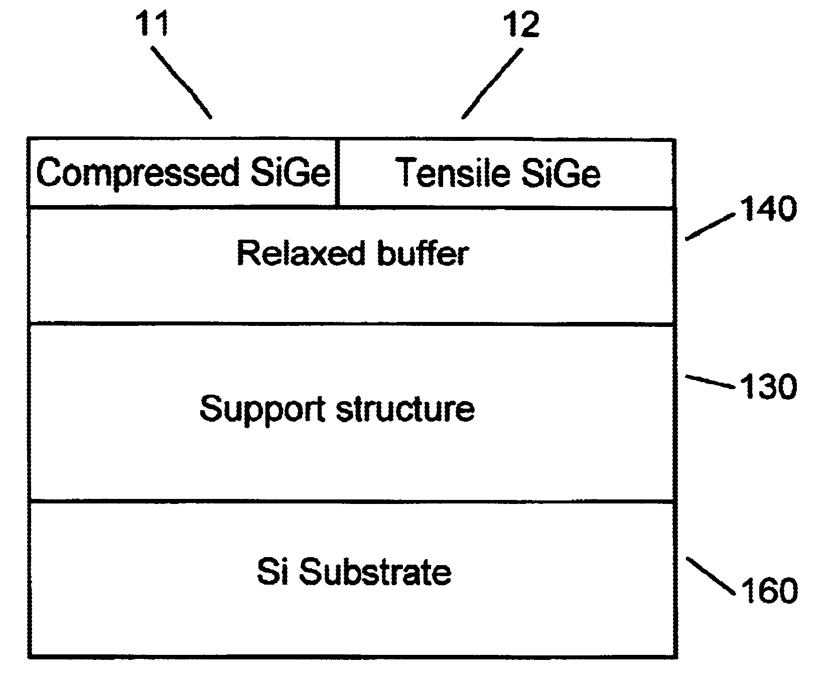
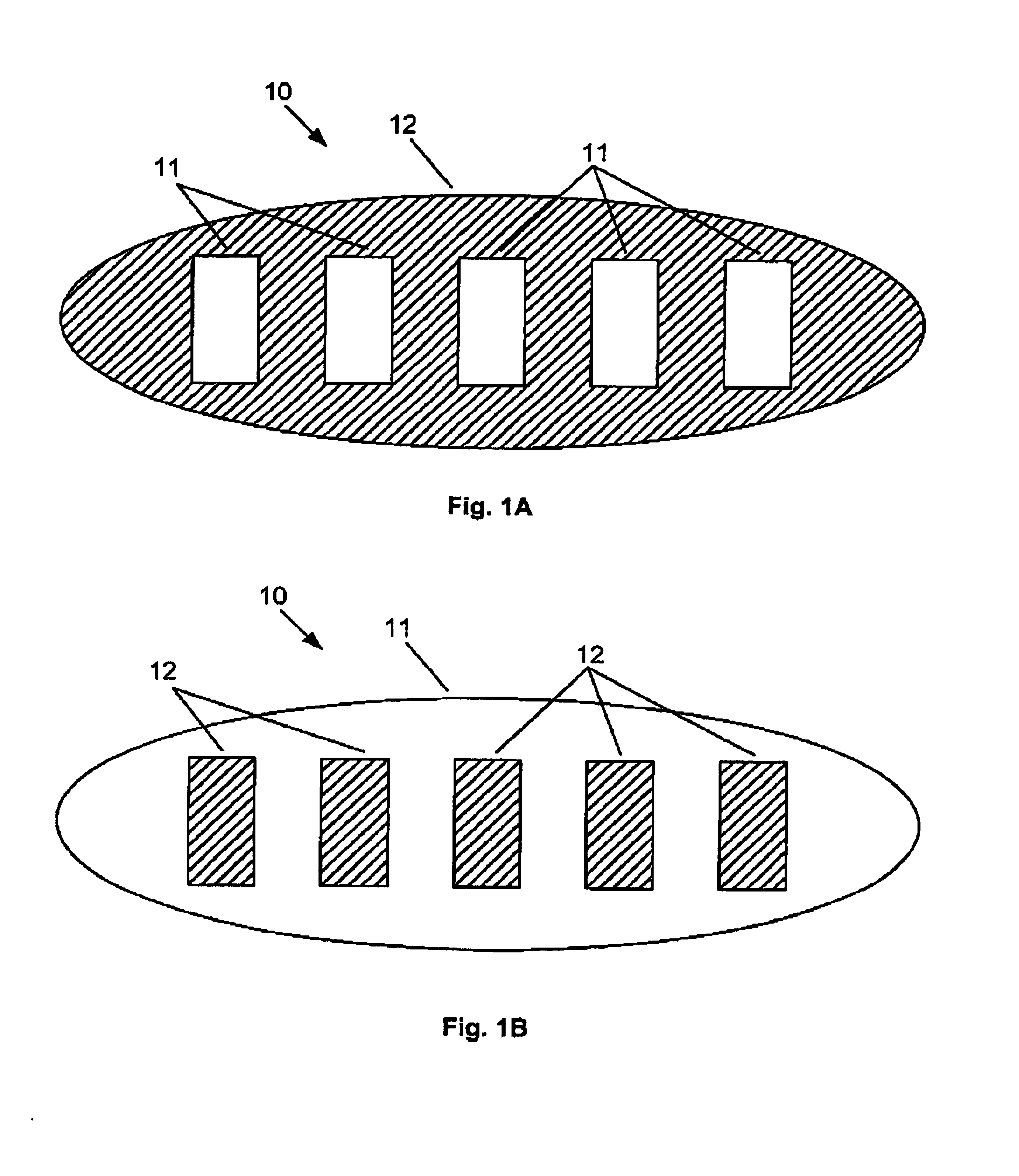
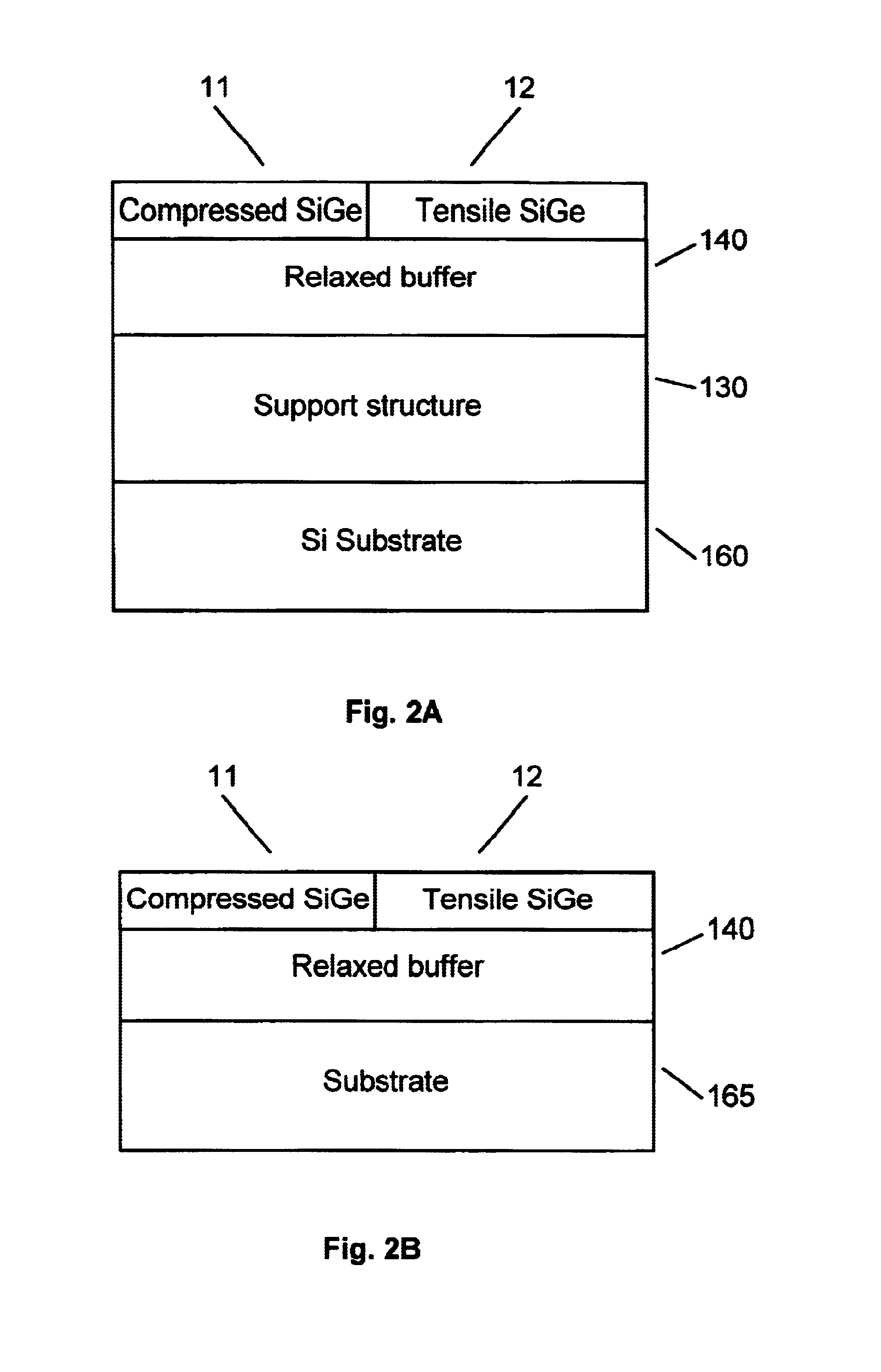
[0054]FIG. 1 shows a top view of crystalline layers 10 having a tensilely strained SiGe portion and a compressively strained SiGe portion. FIG. 1A shows an embodiment, 10, where the compressively strained SiGe portion 11 occupies essentially a plurality of island regions in a tensilely strained SiGe portion 12. This configuration is typically the result of the fabrication method where a uniformly deposited tensilely strained SiGe is opened up and the compressively strained SiGe is then grown in the openings. FIG. 1B shows an alternate preferred embodiment of the strained crystalline layer 10 where the tensilely strained SiGe portion 12 occupies essentially a plurality of island regions in a compressively strained SiGe portion 11. The configuration of FIG. 1B is typically the result of the fabrication method where a uniformly deposited compressively strained SiGe is opened up and the tensilely strained SiGe is then grown in the openings. It is always true that the compressively strai...


PUM


Abstract

A strained crystalline layer having a tensilely strained SiGe portion and a compressively strained SiGe portion is disclosed. The strained crystalline layer is epitaxially bonded, or grown, on top of a SiGe relaxed buffer layer, in a way that the tensilely strained SiGe has a Ge concentration below that of the SiGe relaxed buffer, and the compressively strained SiGe has a Ge concentration above that of the SiGe relaxed buffer. The strained crystalline layer and the relaxed buffer can reside on top a semi-insulator substrate or on top of an insulating divider layer. In some embodiments the tensile SiGe layer is pure Si, and the compressive SiGe layer is pure Ge. The tensilely strained SiGe layer is suited for hosting electron conduction type devices and the compressively strained SiGe is suited for hosting hole conduction type devices. The strained crystalline layer is capable to seed an epitaxial insulator, or a compound semiconductor layer.

Description

FIELD OF THE INVENTION[0001]The present invention relates to strained crystalline semiconductor layers in the field of microelectronics. In particular it teaches the combination of tensilely and compressively strained SiGe regions in the same thin layer, having enhanced carrier mobilities for both electrons and holes. The invention also relates to these strained layers on top of a scalable insulating divider layer, which is optimized for parasitic capacitance and thermal heating resulting in high speed and low noise device operations. The invention further teaches devices hosted in these layers, which can operate from 400° K to 5° K, and teaches processors functioning with such devices. The invention also relates to methods of fabricating such strained SiGe layers and the devices therein.BACKGROUND OF THE INVENTION[0002]Today's integrated circuits include a vast number of devices housed in a semiconductor. Smaller devices are the key to enhance performance and to increase reliabilit...

Claims


Application Information

Patent Timeline
Patent Type & Authority Patents(United States)
IPC IPC(8): H01L29/66H01L21/762H01L29/778H01L21/70H01L29/10H01L29/02H01L21/8238H01L27/085H01L21/84H01L27/092H01L21/20
CPCH01L21/02381H01L21/0245H01L21/02488H01L21/02502H01L21/02505H01L21/02532H01L21/02538H01L21/76254H01L21/823807H01L21/84H01L27/092H01L29/1054H01L29/7782
Inventor CHU, JACK OON
Owner SAMSUNG ELECTRONICS CO LTD
Why Eureka
Try Eureka