

Multilayer structure for absorbing electromagnetic wave and manufacturing method thereof
a technology of electromagnetic waves and multi-layer structures, which is applied in the direction of synthetic resin layered products, transportation and packaging, and other domestic articles, which can solve the problems of increasing the amount of electromagnetic waves emitted and leaked from these electronic devices, affecting the organization and function of human cells, and being too thick to be used for portable, thin-and-light electronic devices such as mobile phones
- Summary
- Abstract
- Description
- Claims
- Application Information
AI Technical Summary
Problems solved by technology
Method used
Image

Examples
first embodiment
[0024
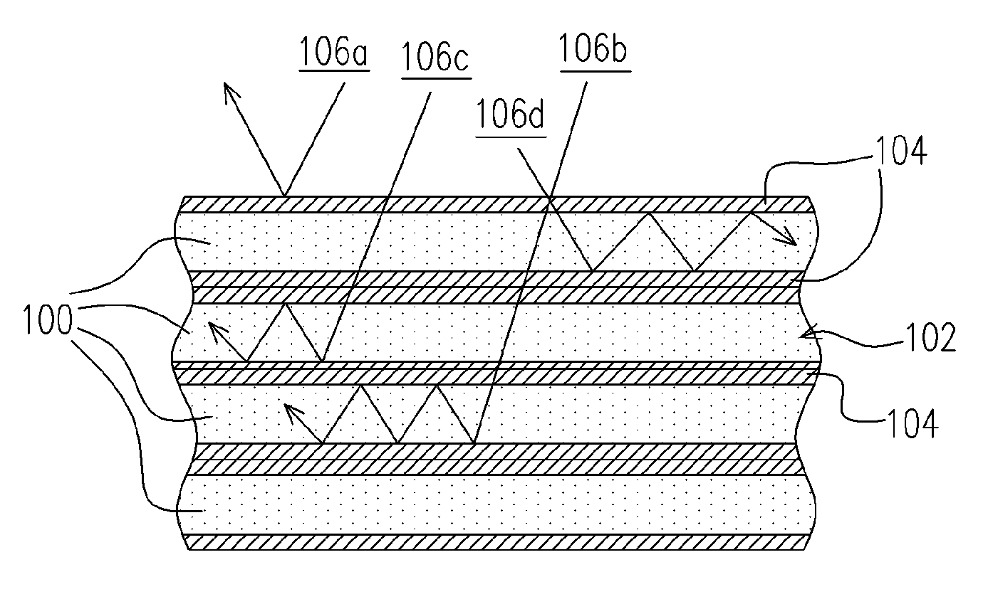
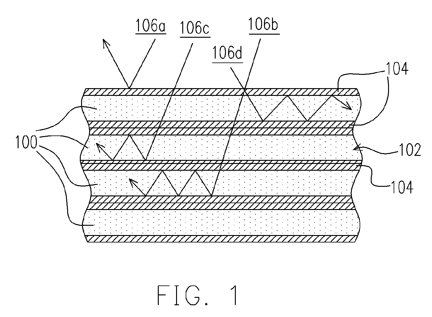
[0025]FIG. 1 is a cross-sectional view of the multilayer film structure for absorbing electromagnetic wave of a first embodiment of the invention.
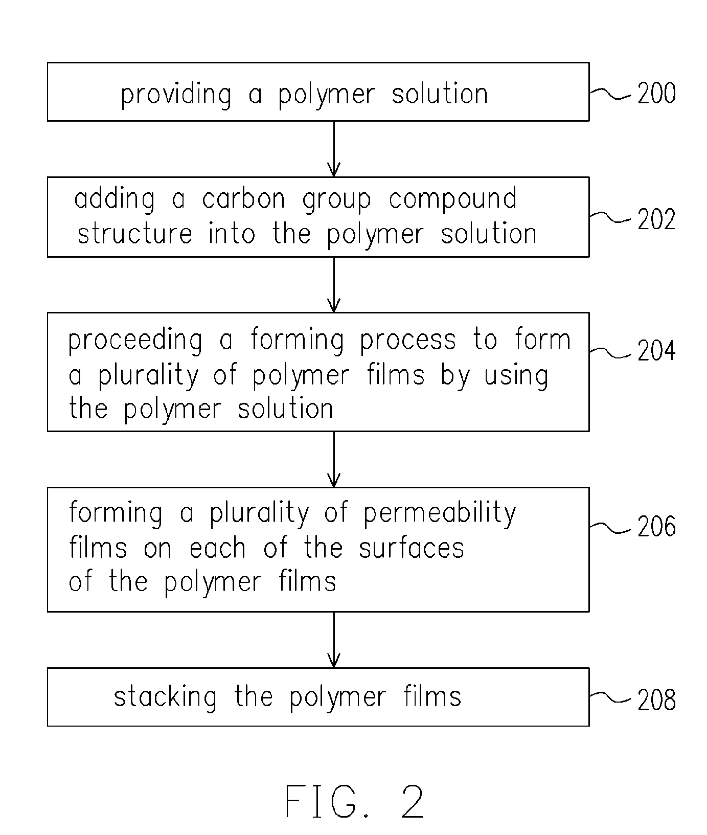
[0026]Referring to FIG. 1, a multilayer film structure for absorbing electromagnetic wave of the invention including a plurality of polymer films 100 and a plurality of permeability films 104. The material of polymer films 100 includes, but not limited to, polyethylene or another polymers. The polymer films 100 have a multi-film stacking structure and at least one of the polymer films 100 is composed of a carbon group compound structure 102. The carbon group compound structure 102 includes, for example but not limited to, a carbon fiber or a carbon containing particle, and the carbon containing particle includes a silicon carbide particle or a nanolevel particle. The permeability films 104 are formed on each surface of the polymer films 100. Therefore, when electromagnetic waves 106a, 106b, 106c and 106d are emitted, the direction of ...
second embodiment
[0030
[0031]FIG. 3 is a sketch illustrating an anti-electromagnetic wave device of a second embodiment of the present invention.
[0032]Referring to FIG. 3, the anti-electromagnetic wave device of the invention is applicable for absorbing the electromagnetic wave emitted from the main body 300 having a cover 302. The feature of the embodiment is that a plurality of polymer films 310 having a multi-film stacking structure are attached to an inner side of the cover 302. The polymer films 310 are composed of a carbon group compound structure 312, and a plurality of permeability films 314 are formed on each surface of the polymer films 310. Moreover, the materials and characteristics are the same as that of the multilayer film structure for absorbing electromagnetic wave described in the first embodiment. However, the cover of the main body will be changed when the present invention is provided for various fields of applications. Therefore, the cover of the main body of the present inventi...
PUM
| Property | Measurement | Unit |
|---|---|---|
| thickness | aaaaa | aaaaa |
| total thickness | aaaaa | aaaaa |
| permeability | aaaaa | aaaaa |
Abstract
Description
Claims
Application Information