Film forming method and apparatus

a film and forming technology, applied in the direction of coatings, chemical vapor deposition coatings, metallic material coating processes, etc., can solve the problems of poor time responsiveness in controlling an on/off of energy supply, deterioration of step coverage performance, and gas phase reaction, and achieve high step coverage

Inactive Publication Date: 2007-06-14
TOKYO ELECTRON LTD
View PDF3 Cites 280 Cited by
  • Summary
  • Abstract
  • Description
  • Claims
  • Application Information

AI Technical Summary

Benefits of technology

[0019] It is, therefore, an object of the present invention to provide a film forming method capable of forming a high-quality thin film having high step coverage on a surface of a substrate without deteriorating a thin film previously formed on the substrate with heat or inflicting plasma damages thereon.

Problems solved by technology

However, in the CVD method for forming a film by continuously supplying a source gas, a reactant gas and energy, certain source gases may cause a gas phase reaction by an excessive activation thereof in a gas phase.
This is because the initial ALD method supplies the thermal energy to a surface of a substrate via the substrate by heating the entire substrate as in the thermal CVD method and, therefore, a time responsiveness in controlling an on / off of energy supply becomes poor (see, e.g., U.S. Pat. No. 4,389,973).
In this method, since the energy is constantly supplied during a source gas supply process, parts of the source gas may ever cause an self-pyrolysis reaction in a gas phase by receiving the thermal energy transferred in the gas phase from the substrate, which leads to a deterioration of the step coverage performance.
Moreover, since the entire substrate is heated constantly during the processing, a solid layer that has been formed by a previous process may be deteriorated by the heat.
Further, since such a method is not a method for supplying energy through a substrate being continuously heated, it is possible to avoid the problem of deteriorating the previously formed solid layer with the heat.
However, the method using as an energy source radicals or ions generated from a plasma has new problems to be described as follows.
Firstly, the excessively high energy of the active species (radicals, ions and electrons) generated from a plasma inflicts a serious physical damage or causes a chemical deterioration on a base layer of a substrate where a film will be formed (see, e.g., A. Grill et al, “Hydrogen plasma effects on ultra low-k porous SiCOH dielectric”, Journal of Applied Physics, vol.
Secondly, the active species also collide against not only the substrate but also an inner surface of an apparatus in contact with the plasma, thereby causing a physical sputtering, which in turn result in impurity incorporation into the surface of the substrate.
Thirdly, since the energy is also supplied by the active species to side chain groups contained in the source gas that are desirably to be removed by the reaction, the side chain groups may be incorporated as undesired impurities into the film.
Fourthly, a potential gradient generated inside the apparatus electrically may destroy fine integrated circuits formed on the substrate.
Fifthly, high energy ultraviolet rays generated from the plasma may deteriorate the base layer of the substrate.
Since, however, a surface of the window becomes dirty during a film forming process, the light is reflected or absorbed and, thus, an intensity of the light reaching the substrate decreases.
Moreover, in case the surface of a processing target substrate is made of a metal, the light is reflected on the surface of the substrate, which hinders the energy supply for the reaction.

Method used


Image

  • Film forming method and apparatus
  • Film forming method and apparatus
  • Film forming method and apparatus

Examples


example 1

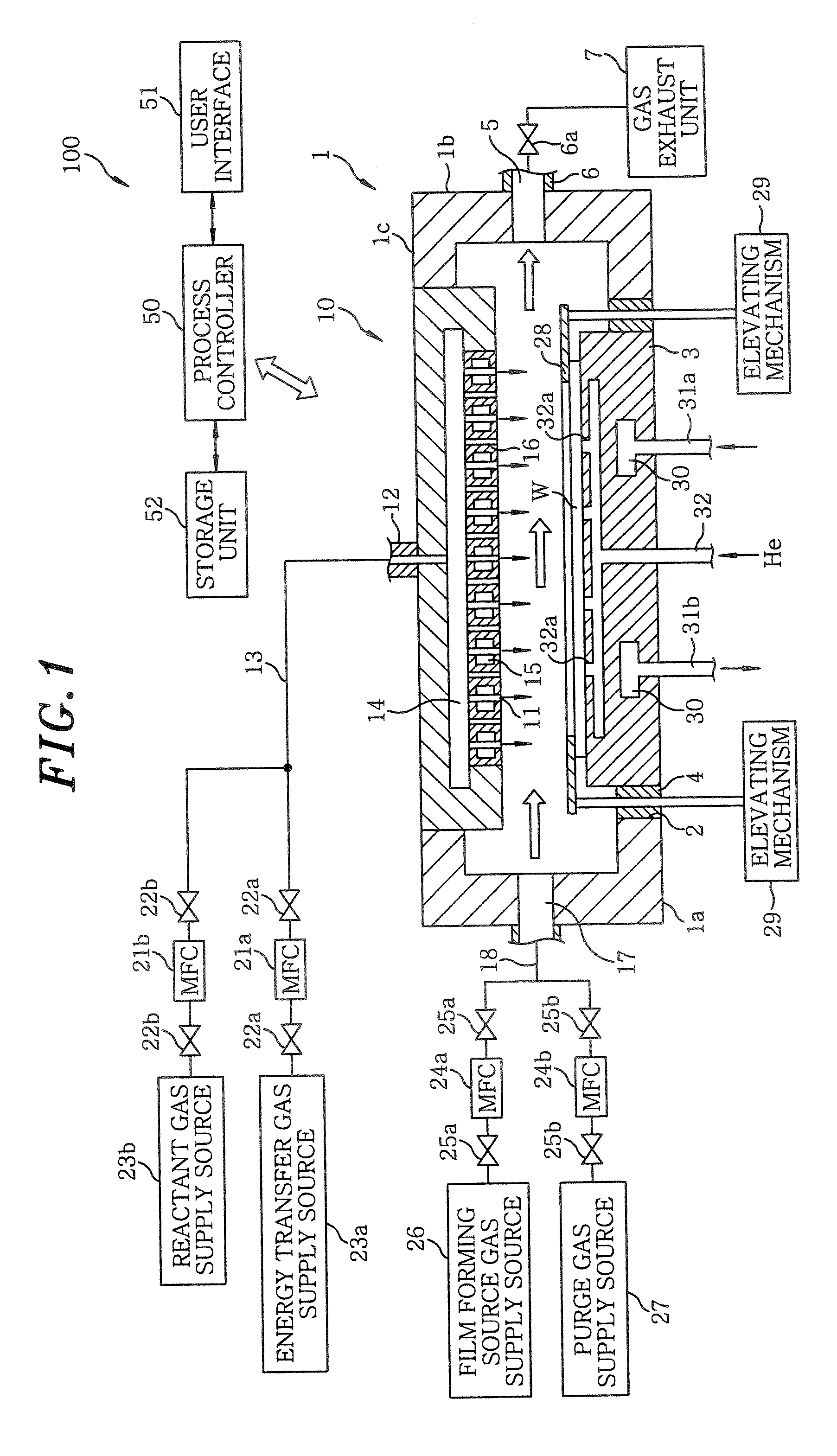
[0150] A wafer W having a diameter of 300 mm was loaded via a transfer robot (not shown) into an aluminum vacuum film forming apparatus having a mounting table whose temperature is controllable as in FIG. 1 and then mounted on the mounting table having a temperature controlled to a preset level of 100° C.

[0151] A liquid source material of Ru(EtCp)2 was introduced into a vaporizer heated to 150° C. and, then, the vaporized gas was introduced into the vacuum film forming apparatus by a carrier gas of Ar. As for an oxidizing gas (reactant gas) O2 was used. Introduced into the chamber 1 were Ru(EtCp)2, Ar serving as a carrier and dilution gas; and O2 serving as a reactant gas and Ar serving as an energy transfer gas heated to a high temperature for a film forming reaction.

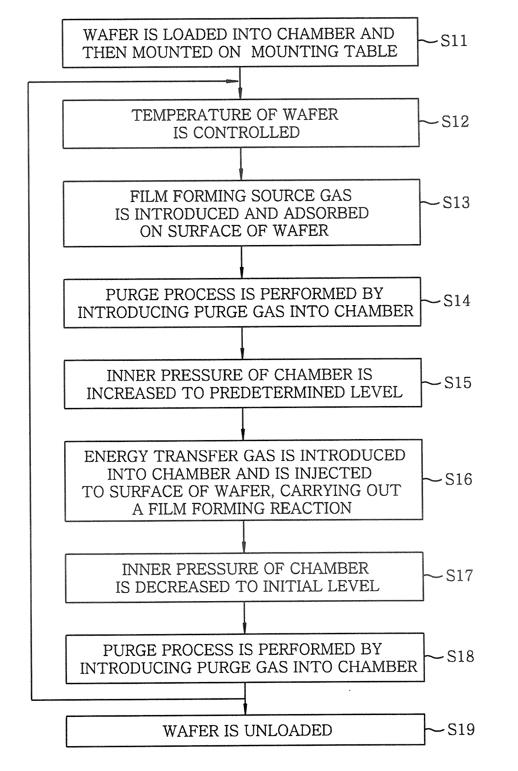
[0152] Next, a film forming process was carried out by performing following steps 1 to 4. FIG. 14 shows a timing chart of the film forming process in this example:

[0153] Step 1;

[0154] Ru(EtCp)2 of 0.1 g / min and the...

example 2

[0162] A wafer W having a diameter of 300 mm was loaded via a transfer robot (not shown) into an aluminum vacuum film forming apparatus having a mounting table whose temperature is controllable as in FIG. 1 and then mounted on the mounting table having a temperature controlled to a preset level of 100° C.

[0163] A liquid source material of Ru(EtCp)2 was introduced into a vaporizer heated to 150° C. and, then, the vaporized gas was introduced into the vacuum film forming apparatus by a carrier gas of Ar. Introduced into the chamber 1 were Ru(EtCp)2, Ar serving as a carrier and dilution gas; and H2 serving as a reactant gas and Ar as an energy transfer gas heated to a high temperature for a film forming reaction.

[0164] Next, a film forming process was carried out by performing following steps 1 to 4. FIG. 15 shows a timing chart of the film forming process in this example:

[0165] Step 1;

[0166] Ru(EtCp)2 of 0.2 g / min and the carrier gas of Ar of 100 mL / min (sccm) were set to flow for...

example 3

[0174] A wafer W having a diameter of 300 mm was loaded via a transfer robot (not shown) into an aluminum vacuum film forming apparatus having a mounting table whose temperature is controllable as in FIG. 1 and then mounted on the mounting table having a temperature controlled to a preset level of 100° C.

[0175] A liquid source material of Ru(EtCp)2 was introduced into a vaporizer heated to 150° C. and, then, the vaporized gas was introduced into the vacuum film forming apparatus by a carrier gas of Ar. Introduced into the chamber 1 were Ru(EtCp)2, Ar serving as a carrier and dilution gas; and Ar serving as an energy transfer gas heated to a high temperature for a film forming reaction.

[0176] Next, a film forming process was carried out by performing following steps 1 to 4. FIG. 16 shows a timing chart of the film forming process in this example:

[0177] Step 1;

[0178] Ru(EtCp)2 of 0.2 g / min and the carrier gas of Ar of 100 mL / min (sccm) were set to flow for 20 seconds while setting...


PUM

PropertyMeasurementUnit
temperatureaaaaaaaaaa
pressureaaaaaaaaaa

Abstract

A film forming method, for depositing a thin film on a surface of a substrate mounted on a mounting table disposed in a vacuum processing chamber, includes an adsorption process for adsorbing a film forming material on the substrate by introducing a source gas into the processing chamber; and a reaction process for carrying out a film forming reaction, after the adsorption process, by introducing an energy transfer gas into the processing chamber and supplying thermal energy to the film forming material adsorbed on the substrate. By repeating the above process, the thin film is formed on the substrate in a layer-by-layer manner.

Description

FIELD OF THE INVENTION [0001] The present invention relates to a film forming method and apparatus; and, more particularly, to a film forming method for forming a desired thin film on a surface of a substrate by using an ALD (atomic layer deposition) method and a film forming apparatus therefor. BACKGROUND OF THE INVENTION [0002] As for a representative film forming method for forming a solid thin film on a surface of a substrate such as a semiconductor wafer or the like, there is known a CVD (chemical vapor deposition) method. When a film is formed by using the CVD method, a source needs to be activated by applying energy to a source gas. Accordingly, there has been employed a CVD method for supplying thermal energy to a source gas through a substrate heated by a heater provided at a mounting table for mounting thereon the substrate or a plasma CVD method for supplying energy of a plasma generated in a space above a substrate by introducing a source gas into the atmosphere thereof....

Claims


Application Information

Patent Timeline
Patent Type & Authority Applications(United States)
IPC IPC(8): H01L21/44
CPCC23C16/16C23C16/18C23C16/34C23C16/452C23C16/45534C23C16/45548C23C16/45557C23C16/46H01L21/28562
Inventor GUNJI, ISAOKAWANO, YUMIKO
Owner TOKYO ELECTRON LTD
Why Eureka
Try Eureka