Method for manufacturing grid side wall of ONO structure

A gate sidewall and manufacturing method technology, applied in semiconductor/solid-state device manufacturing, gaseous chemical plating, coating and other directions, can solve the thickness uniformity difference of semiconductor substrate thickness uniformity, unsatisfactory step coverage, Affect the performance of semiconductor devices and other issues, and achieve the effect of high step coverage, good intra-chip uniformity and inter-chip uniformity

Inactive Publication Date: 2014-01-01
SHANGHAI HUALI MICROELECTRONICS CORP
View PDF3 Cites 0 Cited by
  • Summary
  • Abstract
  • Description
  • Claims
  • Application Information

AI Technical Summary

Problems solved by technology

[0003] With the reduction of device line width (55nm and below) and the improvement of integration, traditional furnace tube TEOS (tetraethyl silicate) process or high temperature thermal oxidation (HTO) and furnace tube DCS-NH3 process are used to make ONO structure When the gate spacer i

Method used


Image

  • Method for manufacturing grid side wall of ONO structure
  • Method for manufacturing grid side wall of ONO structure
  • Method for manufacturing grid side wall of ONO structure

Examples


Example Embodiment

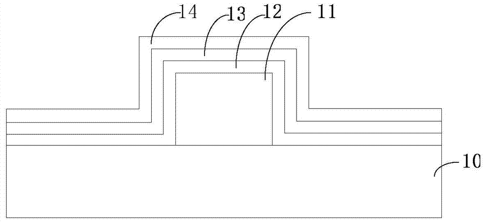
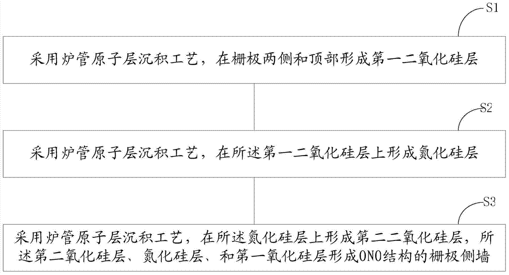
[0028] In the prior art, the first silicon oxide layer and the second silicon oxide layer are made by the furnace tube TEOS process or the furnace tube high temperature thermal oxidation process, and the silicon nitride process is made by the furnace tube DCS NH3 process. The process uniformity is not high, and the step coverage is not good. In order to solve the above problems, the present invention proposes a method for manufacturing the gate side wall structure of the ONO structure. Please refer to figure 2 The flow chart of the manufacturing method of the gate sidewall spacer of the ONO structure in the prior art shown in the prior art, the method includes:

[0029] Step S1, using a furnace tube atomic layer deposition process to form a first silicon dioxide layer on both sides and top of the gate;

[0030] Step S2, using a furnace tube atomic layer deposition process to form a silicon nitride layer on the first silicon dioxide layer;

[0031] Step S3, a furnace tube atomic laye...


PUM


Abstract

The invention provides a method for manufacturing a grid side wall of an ONO structure. The method comprises the step of forming a first silicon dioxide layer on the two sides and the top of a grid by adopting the furnace tube atomic layer deposition technology, the step of forming a silicon nitride layer on the first silicon dioxide layer by adopting the furnace tube atomic layer deposition technology, and the step of forming a second silicon dioxide layer on the silicon nitride layer by adopting the furnace tube atomic layer deposition technology. The grid side wall of the ONO structure is formed by the second silicon dioxide layer, the silicon nitride layer and the first silicon dioxide layer. According to the method, the evenness and the step covering rate of the grid side wall of the ONO structure are improved, and the performance of an ultimately formed semiconductor device is improved.

Description

technical field [0001] The invention relates to the field of semiconductor technology, in particular to a method for manufacturing gate spacers of an ONO structure. Background technique [0002] In the manufacturing process of the semiconductor process, the gate spacer structure plays an important role in protecting the gate and reducing the short channel effect of the device. ONO (first silicon dioxide layer-silicon nitride layer-second silicon oxide layer) structure is an existing ideal gate spacer structure, please refer to figure 1 The schematic diagram of the gate sidewall structure of the ONO structure shown in the prior art. The gate 11 on the semiconductor substrate 10 is sequentially covered with a first silicon oxide layer 12, a silicon nitride layer 13 and a second silicon nitride layer 14, wherein the silicon nitride layer 13 has a higher density and strength, and can It can effectively prevent the diffusion of water vapor and sodium ions, and is an ideal gate ...

Claims


Application Information

Patent Timeline
IPC IPC(8): H01L21/28H01L21/285
CPCH01L21/285C23C16/345C23C16/402C23C16/45529
Inventor 江润峰戴树刚
Owner SHANGHAI HUALI MICROELECTRONICS CORP
Why Eureka
Try Eureka