Memory block erasing in a flash memory device

a flash memory device and memory block technology, applied in the field of memory devices, can solve the problems of reducing unable to guarantee that some cells have not been over-erased, and unable to erase errors, so as to reduce the time of erasing a memory device

Active Publication Date: 2005-12-13
MICRON TECH INC
View PDF14 Cites 96 Cited by
  • Summary
  • Abstract
  • Description
  • Claims
  • Application Information

AI Technical Summary

Problems solved by technology

At the end of the erase operation, there is no guarantee that some cells have not been over-erased.
In the latter case, an erase error has occurred.
Performing all of these steps to erase a block of memory makes the erase operation of a flash memory device a time consuming operation.

Method used


Image

  • Memory block erasing in a flash memory device
  • Memory block erasing in a flash memory device
  • Memory block erasing in a flash memory device

Examples


Embodiment Construction

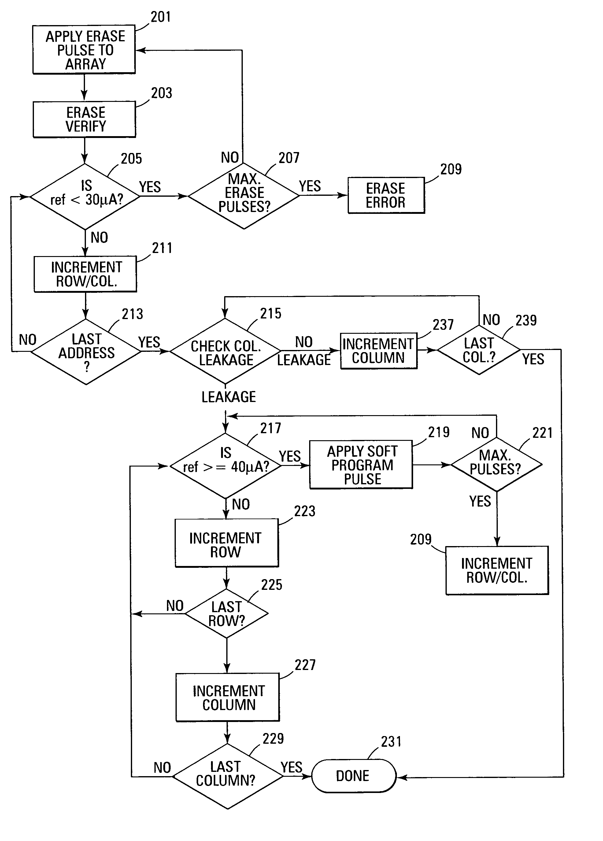
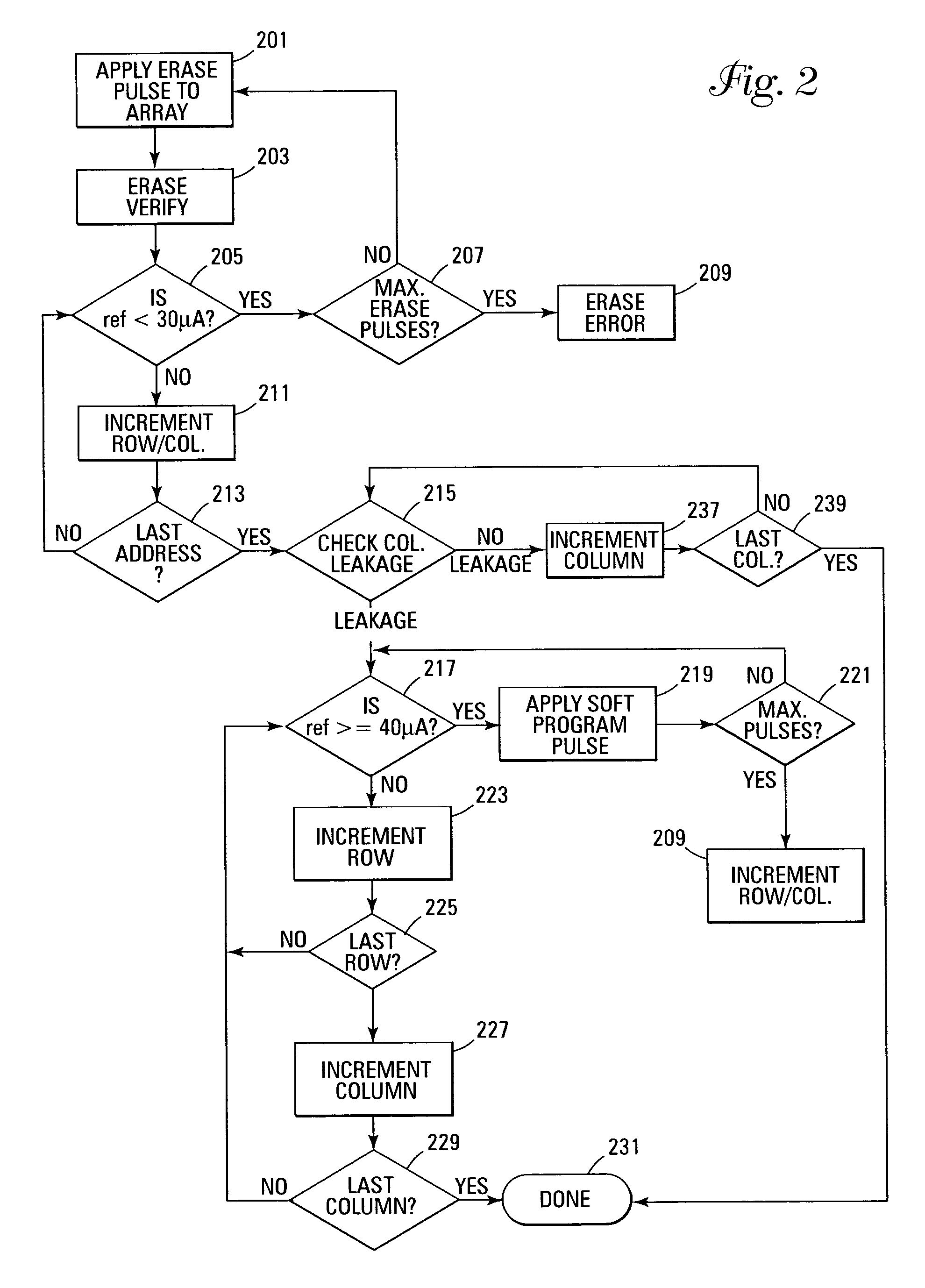
[0016]In the following detailed description of the invention, reference is made to the accompanying drawings that form a part hereof, and in which is shown, by way of illustration, specific embodiments in which the invention may be practiced. In the drawings, like numerals describe substantially similar components throughout the several views. These embodiments are described in sufficient detail to enable those skilled in the art to practice the invention. Other embodiments may be utilized and structural, logical, and electrical changes may be made without departing from the scope of the present invention. The following detailed description is, therefore, not to be taken in a limiting sense, and the scope of the present invention is defined only by the appended claims and equivalents thereof.

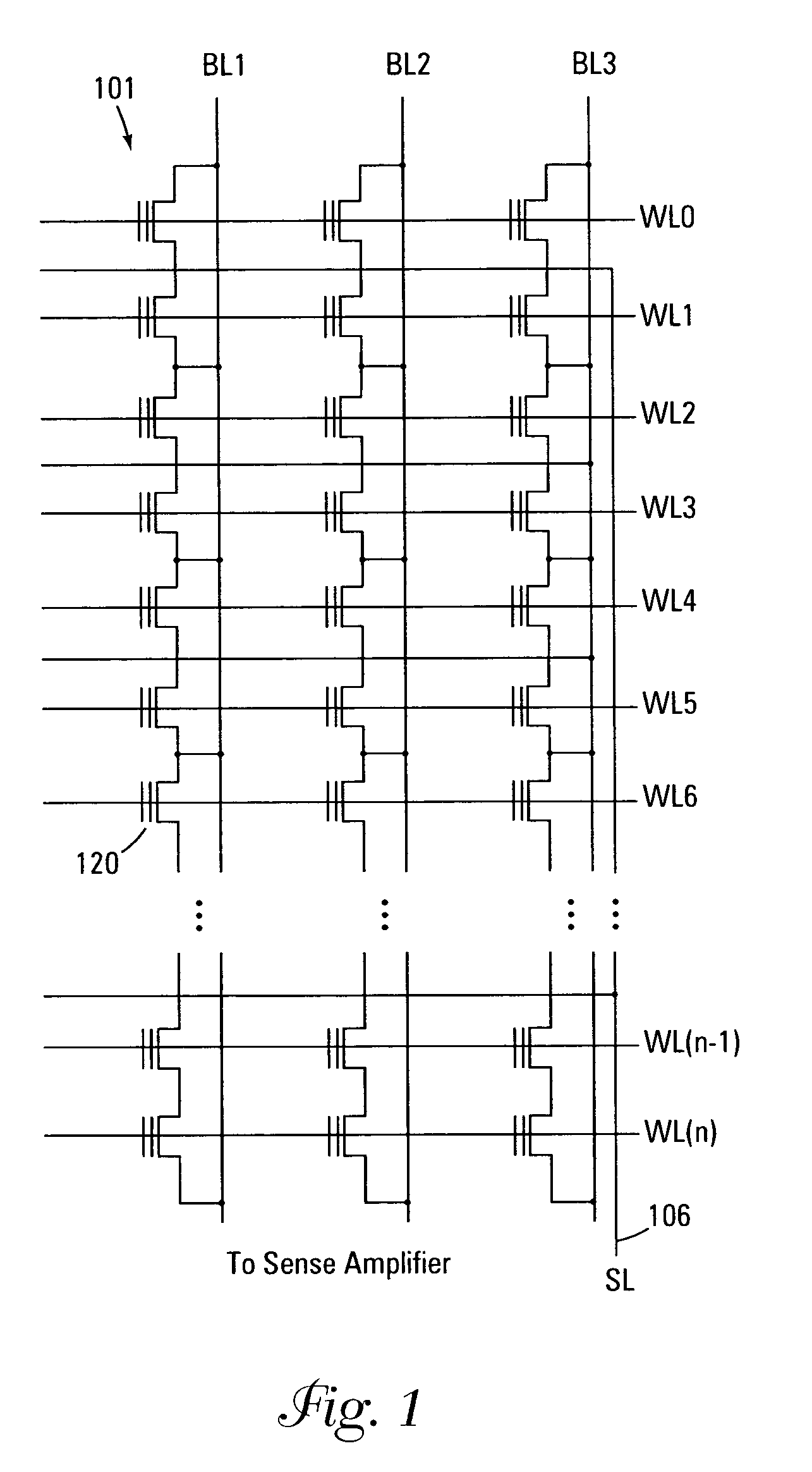
[0017]FIG. 1 illustrates a typical NOR-type flash memory array in accordance with the method of FIG. 1. The memory is comprised of an array 101 of floating gate cells 120 arranged in rows and co...


PUM


Abstract

An erase pulse is applied to the memory block to be erased. An erase verification operation is performed to verify that each memory cell of the memory block is erased. If a memory cell has a current less than a first sense amplifier current reference level, additional erase pulses are applied to that cell until either the erase current is in the range of 30–40 μA or a maximum quantity of erase pulses have been applied. A leakage check is performed to determine if any cells have been overerased. If a cell has an erase current greater than or equal to a second sense amplifier current reference level, soft programming pulses are applied to the cell until either its erase current is less than the second reference level or a maximum quantity of soft program pulses have been applied.

Description

TECHNICAL FIELD OF THE INVENTION[0001]The present invention relates generally to memory devices and in particular the present invention relates to erasing flash memory devices memory devices.BACKGROUND OF THE INVENTION[0002]Memory devices are typically provided as internal, semiconductor, integrated circuits in computers or other electronic devices. There are many different types of memory including random-access memory (RAM), read only memory (ROM), dynamic random access memory (DRAM), synchronous dynamic random access memory (SDRAM), and flash memory.[0003]A flash memory is a type of memory that can be erased and reprogrammed in blocks instead of one byte at a time. A typical flash memory comprises a memory array, which includes a large number of memory cells. Each of the memory cells includes a floating gate field-effect transistor capable of holding a charge. The cells are usually grouped into blocks. Each of the cells within a block can be electrically programmed in a random ba...

Claims


Application Information

Patent Timeline
Patent Type & Authority Patents(United States)
IPC IPC(8): G11C11/34G11C16/04G11C16/16G11C16/34
CPCG11C16/16G11C16/3404G11C16/3409G11C16/344G11C16/345
Inventor ABEDIFARD, EBRAHIMROOHPARVAR, FRANKIE F.
Owner MICRON TECH INC
Why Eureka
Try Eureka