Method for forming a dielectric layer in a semiconductor device

a semiconductor device and dielectric layer technology, applied in the direction of coatings, transistors, chemical vapor deposition coatings, etc., can solve the problems of affecting the dielectric effect, affecting the efficiency of the dielectric layer, and it is difficult to completely remove the oxygen vacancies, so as to achieve low current leakage values and high insulation breakdown voltage

Inactive Publication Date: 2005-12-27
SK HYNIX INC
View PDF7 Cites 2 Cited by
  • Summary
  • Abstract
  • Description
  • Claims
  • Application Information

AI Technical Summary

Problems solved by technology

Recently, however, much effort has been spent looking for new materials that have better characteristics than SiO2 with which to form gate insulators and the like.
Unfortunately, however, Ta2O5 contains impurities as well.
Such elements can cause current leakage, and thus impair the dielectric effect.
Nevertheless, it is impossible to remove the oxygen vacancies completely.
Accordingly, Ta2O5 gate insulator formation processes becomes complicated owing to a low temperature oxidation processes such as plasma annealing and UV-O3 annealing preformed in-situ or ex-situ.
As a result, the Ta2O5 layer loses the merit of metal-based oxide layer having a high dielectric constant.
Alternately, a low temperature oxidation process may be introduced to prevent the Si—Tax—Ox compound from converting to SiO2 Such processes do not crystallize the amorphous Ta2O5 layer, however, making it difficult to obtain a metal based Ta2O5 layer having a high dielectric constant.

Method used


Image

  • Method for forming a dielectric layer in a semiconductor device
  • Method for forming a dielectric layer in a semiconductor device
  • Method for forming a dielectric layer in a semiconductor device

Examples


Embodiment Construction

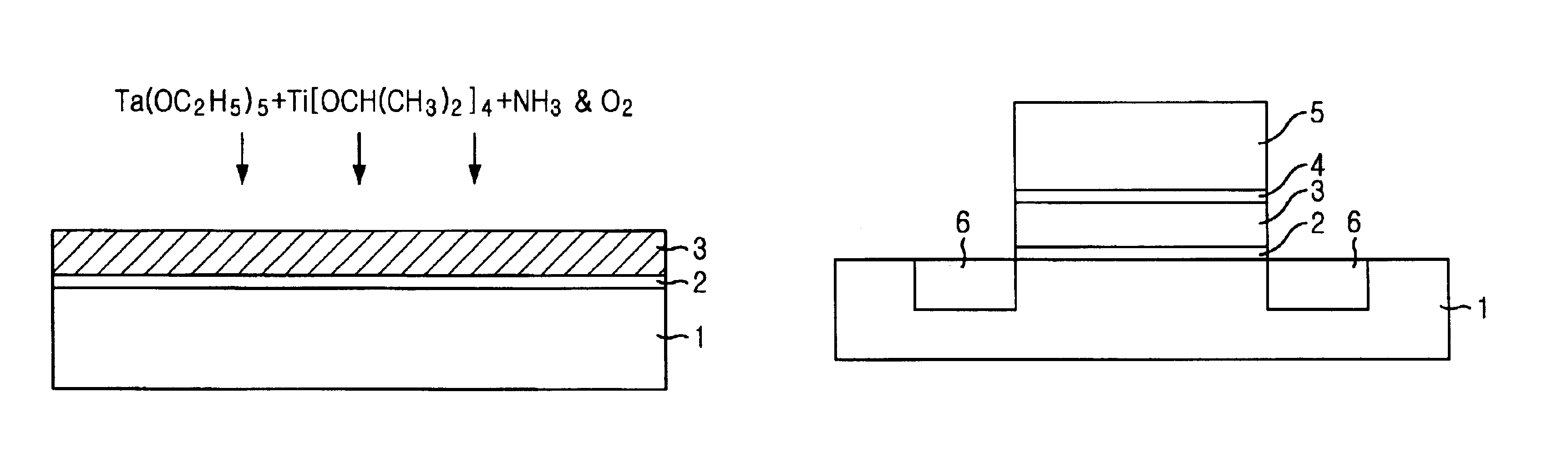
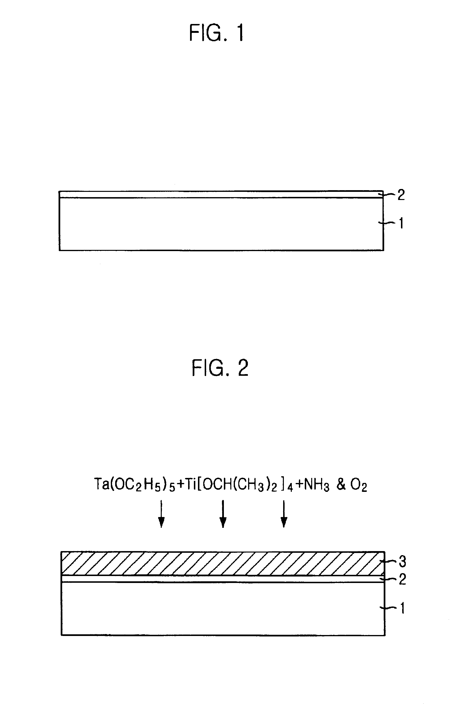
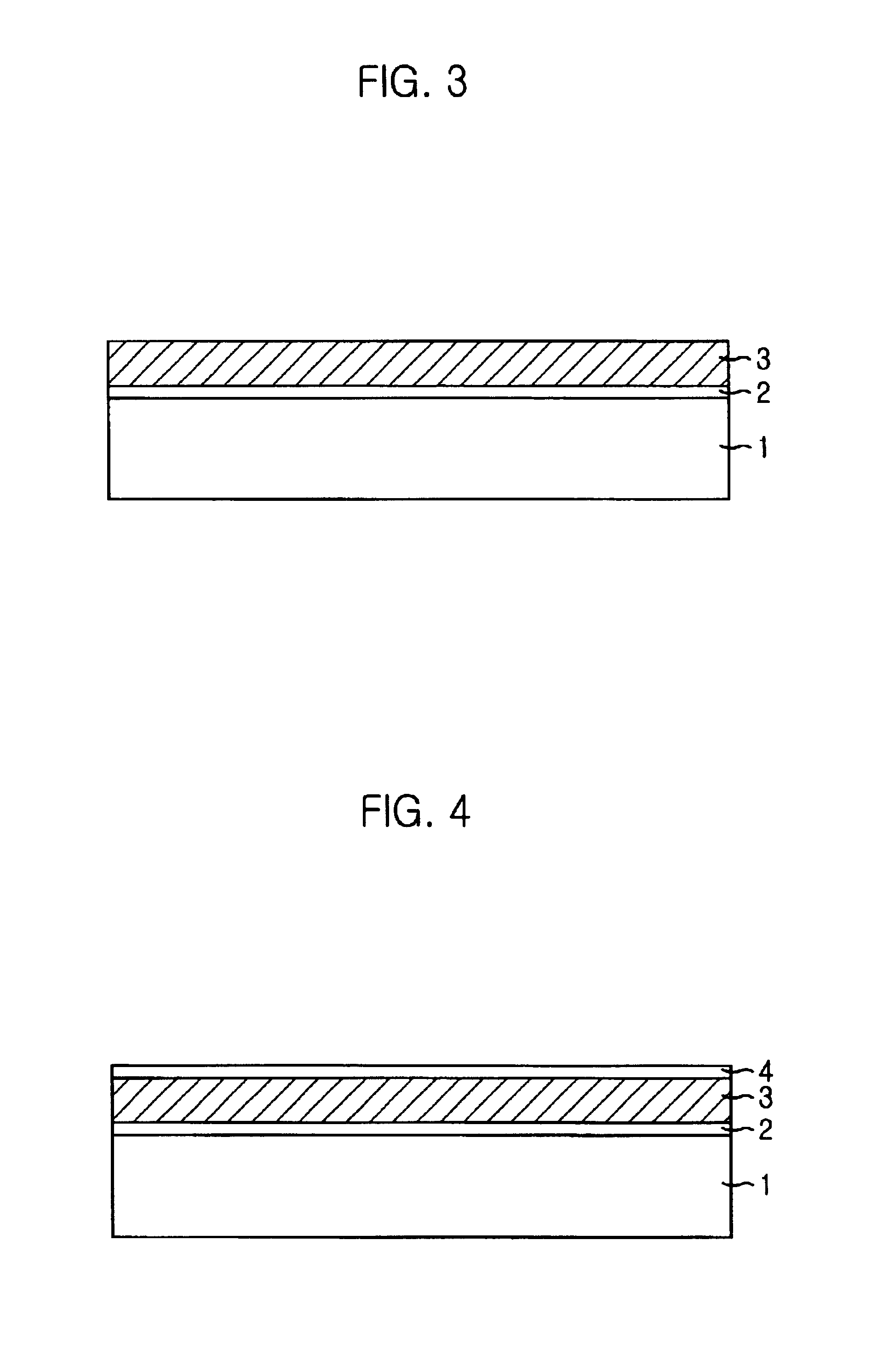
[0015]Other embodiments and aspects of the present invention will become apparent from the following description, with reference to the accompanying drawings, which is set forth hereinafter. All units of temperature expressed herein are in degrees centigrade (°C.); all units of thickness are in angstroms (Å), unless otherwise indicated. In the formula, (TaO)1−x(TiO)xN, as used herein, x ranges from about 0.01 to about 0.09.

[0016](TaO)1−x(TiO)xN, wherein x ranges from about 0.01 to about 0.09, may be used to form a gate electrode in accordance with the present invention. (TaO)1−x(TiO)xN, wherein x ranges from about 0.01 to about 0.09, has a dielectric constant of above 40, which has a higher dielectric constant than SiO2. (SiO2 has a dielectric constant of 3.85.) In addition (TaO)1−x(TiO)xN (x defined above) has a dielectric intensity that is higher than Ta2O5. This is because (TaO)1−x(TiO)xN (x defined above) is composed of covalently bonded Ta—O—N compounds and Ti—O—N compounds, wh...


PUM

PropertyMeasurementUnit
mole ratioaaaaaaaaaa
temperatureaaaaaaaaaa

Abstract

The present invention provides a method for forming an improved dielectric layer for semiconductor devices such as gate structures and capacitors. The method utilizes a layer of (TaO)1−x(TiO)xN (x defined herein) as a substitute for SiO2, together with one or more additional procedures to minimize or prevent channel leakage and other problems that can minimize the performance of the structure.

Description

FIELD OF THE INVENTION[0001]The present invention relates to a method for fabricating a highly integrated semiconductor device; and, more particularly, to a method for forming a dielectric layer with (TaO)1−x(TiO)xN (0.01≦x≦0.09) having a high dielectric constant.CROSS REFERENCE TO RELATED APPLICATIONS[0002]This application is related to, and claims the benefits of priority of, Application No.: 2001-74334, filed Nov. 27, 2001, in the Republic of Korea, the contents of which are incorporated herein in by reference their entirety.BACKGROUND OF THE INVENTION[0003]High dielectric materials have many uses in semiconductor devices. Mainly, high dielectric materials are used to form dielectric layers of capacitors and gate insulators of transistors.[0004]Conventionally, layers of SiO2, having a dielectric constant of 3.85, have been used to form gate insulators. Recently, however, much effort has been spent looking for new materials that have better characteristics than SiO2 with which to ...

Claims


Application Information

Patent Timeline
Patent Type & Authority Patents(United States)
IPC IPC(8): C23C16/30H01L21/283H01L21/28H01L21/314H01L21/316H01L21/318H01L21/334H01L21/822H01L21/8242H01L27/04H01L27/108H01L29/51H01L29/78
CPCC23C16/308H01L21/28185H01L21/28194H01L21/28202H01L21/3143H01L21/31604H01L29/513H01L29/518H01L29/511H01L21/02299H01L21/02205H01L21/02183H01L21/02194H01L21/02271H01L21/02186H01L21/18H01L21/02337H01L21/0234H01L21/02356
Inventor JOO, KWANG-CHULKIM, JAE-OK
Owner SK HYNIX INC
Why Eureka
Try Eureka