Checking method and checker for thin film loading band for encasulating electronic part

A technology of electronic components and inspection devices, which is applied in the direction of using optical devices, measuring devices, electrical components, etc., and can solve the problems of easy leakage, judgment deviation, leakage of defective electronic component packaging film carrier tape, etc.

Inactive Publication Date: 2006-09-27
MITSUI MINING & SMELTING CO LTD
View PDF0 Cites 2 Cited by
  • Summary
  • Abstract
  • Description
  • Claims
  • Application Information

AI Technical Summary

Problems solved by technology

[0006] However, since such marks are provided near both ends of the electronic component packaging film carrier tape, it is easy to miss them in visual inspection by humans, and since it is based on human judgment, it is difficult to judge In any case, there are deviations, it is difficult to perform stable quality inspection, and there is a danger of missing defective film carrier tapes for electronic component packaging

Method used


Image

  • Checking method and checker for thin film loading band for encasulating electronic part
  • Checking method and checker for thin film loading band for encasulating electronic part
  • Checking method and checker for thin film loading band for encasulating electronic part

Examples


Embodiment Construction

[0019] Hereinafter, embodiments (Examples) of the present invention will be described with reference to the drawings.

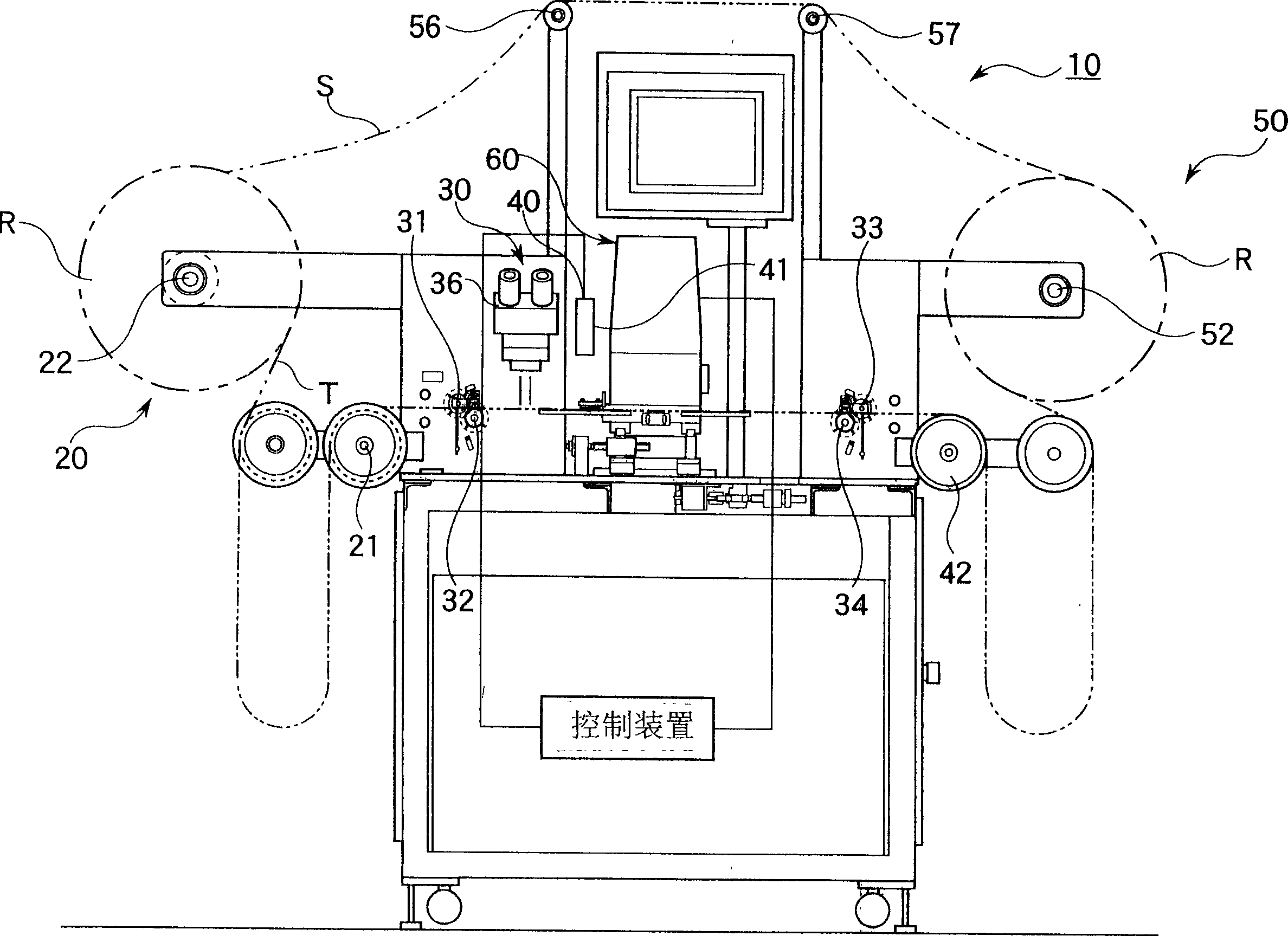
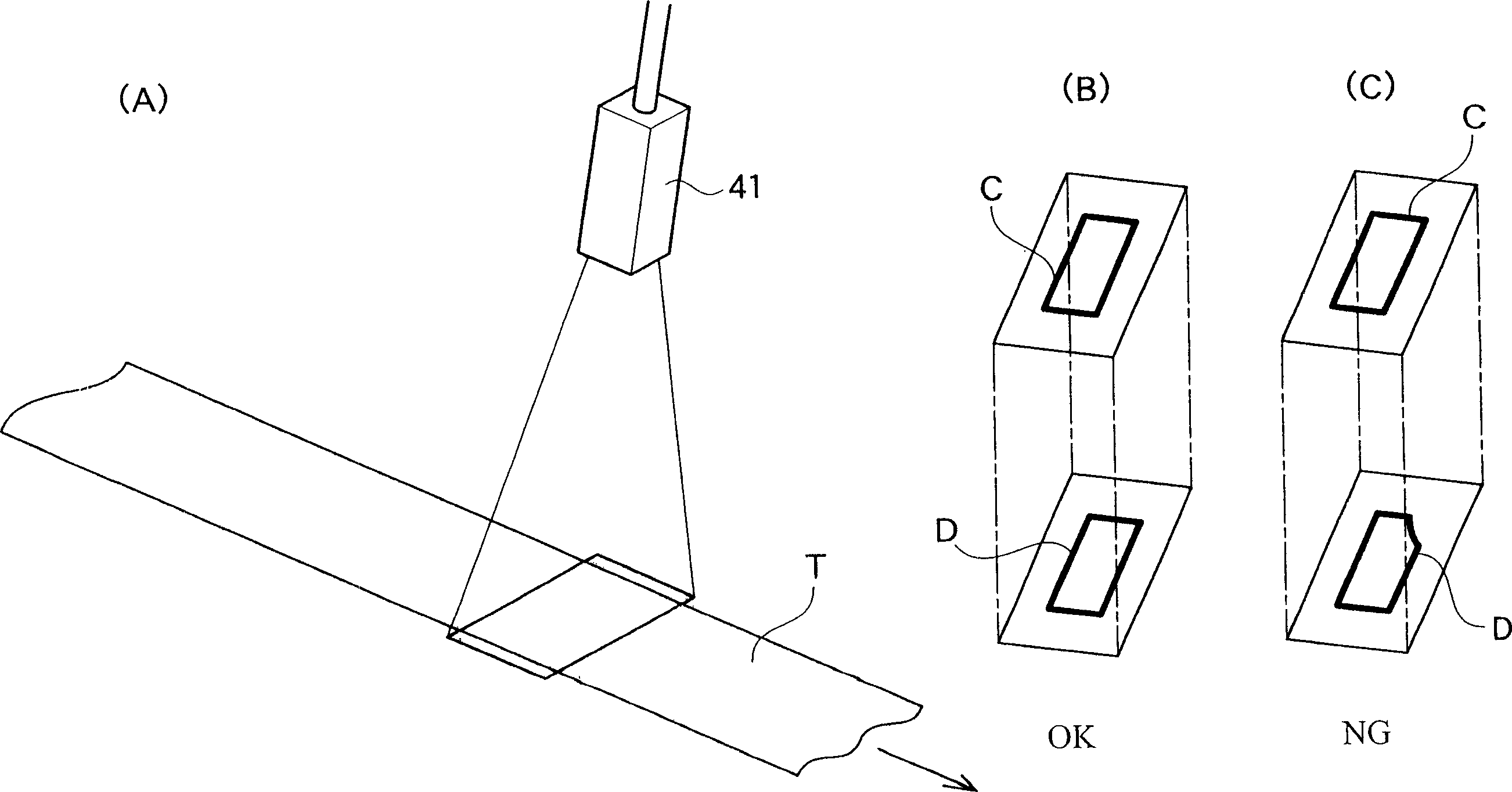
[0020] figure 1 It is a front view of the inspection apparatus of the film carrier tape for electronic component packaging of this invention.

[0021] Such as figure 1 As shown, 10 represents the entire inspection device of the film carrier tape for packaging electronic components of the present invention.

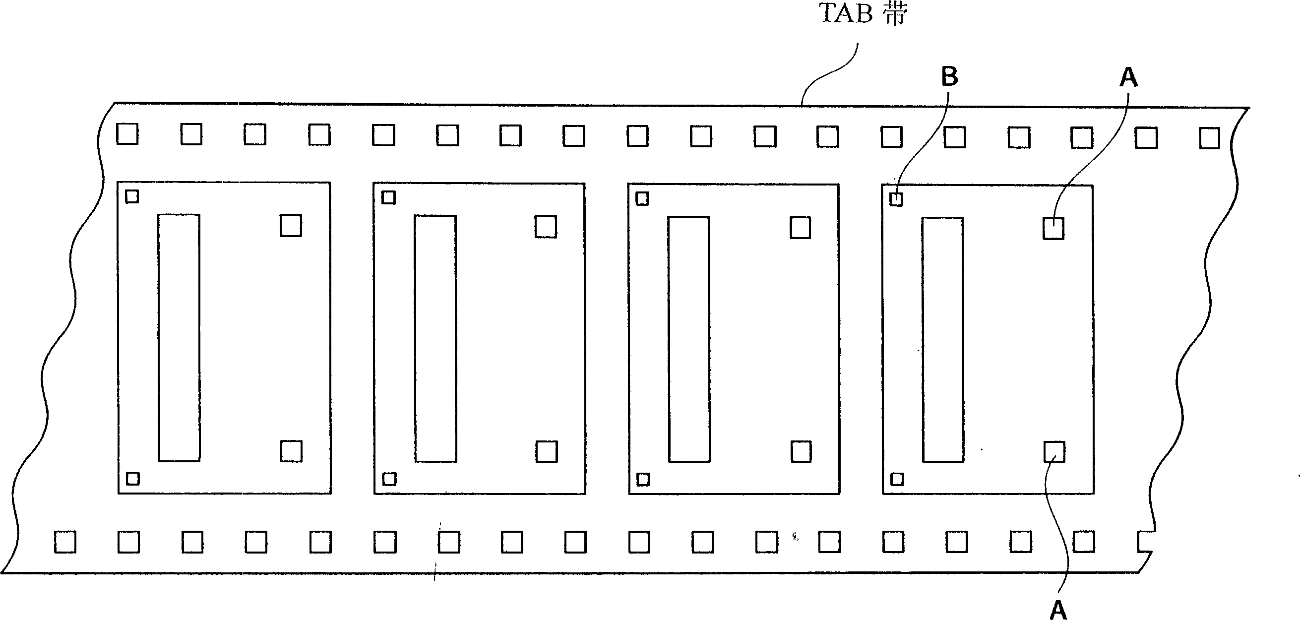
[0022] Such as figure 1 As shown, the inspection device 10 of a film carrier tape for packaging electronic components (hereinafter referred to as "inspection device 10") includes a sending device 20, an inspection unit 30, a marking unit 60, and a winding device 50. In the delivery device 20, there is a film carrier tape for packaging electronic components (hereinafter referred to as "film carrier tape"), and the film carrier tape T, which has completed the manufacturing process, is mounted on the delivery drive shaft 22 through a reel R wound on a separa...


PUM


Abstract

The present invention relates to an inspection method and an apparatus of film carrier tape for mounting electronic parts, which are used for inspecting poor marks such as alignment mark for determining the assembling position in mounting IC electronic parts, a land for holding the tape without additional procedures and labor. The method and the apparatus of the present invention could be carried out at a low cost, in short inspecting time, and in excellent accuracy. The inspection method of film carrier tape for mounting electronic parts of the present invention comprises the steps of comparing a pattern shape of a mark pre-stored in a memory with a pattern shape of a mark input to a sensor, then judging as a poor mark if a consistency between the two pattern shapes is below a predetermined threshold value.

Description

Technical field [0001] The present invention relates to a method for inspecting a film carrier tape for electronic component packaging and an inspection device for a film carrier tape for electronic component packaging. It is used to detect the film carrier tape for electronic component packaging [TAB (Tape Automated Bonding; carrier tape automatic bonding) tape, T -BGA (Tape Ball Grid Array) tape, CSP (Chip Size Package) tape, ASIC (Application Specific Integrated Circuit; application specific integrated circuit) tape, etc.], COF (Chip On Film) ; Film-based chip), bimetal (double-sided wiring) tape, multilayer wiring tape, etc. (hereinafter referred to as "film carrier tape for electronic component packaging") defects in alignment marks, pads, etc. Background technique [0002] With the development of the electronics industry, the demand for printed circuit boards for packaging electronic components such as ICs (Integrated Circuits) and LSIs (Large Scale Integrated Circuits) has...

Claims


Application Information

Patent Timeline
Patent Type & Authority Patents(China)
IPC IPC(8): H01L21/66H01L21/60G01B11/24
Inventor 长谷川浩司
Owner MITSUI MINING & SMELTING CO LTD
Why Eureka
Try Eureka