Method and system for partial-scan testing of integrated circuits

a technology of integrated circuits and partial scans, applied in the field of partial scan testing of integrated circuits, can solve the problems of lower yield of usable chips, higher production costs, and failure of integrated circuit scan testing, so as to reduce the cost of manufacturing ic, and increase the yield of ic batch

Inactive Publication Date: 2006-01-03
MICRON TECH INC
View PDF17 Cites 2 Cited by
  • Summary
  • Abstract
  • Description
  • Claims
  • Application Information

AI Technical Summary

Benefits of technology

[0008]The present invention solves the above-identified problems and allows any number of functional blocks within the IC to be isolated, and therefore logically removed from scan testing, allowing the rest of the IC to be tested normally. By isolating a failing block and continuing testing, the entire IC does not have to be scrapped. It could be packaged and sold at a reduced cost without the failing functionality. This would then increase the yield of the IC batch, and lower the costs of producing the IC. For example, if a system on a chip IC were to fail during full scan testing, and the failure was isolated down to a single functional block, for example an interface, the chip could be packaged and resold into markets that do not require the particular interface.

Problems solved by technology

The failure of a single transistor within one of these complex blocks will cause an integrated circuit to fail scan testing.
As a result, the chip will be scrapped, resulting in a lower yield of usable chips, as well as higher production costs.
Therefore, in such an arrangement, if a failure is detected during testing of block A, the entire integrated circuit 10 must be scrapped because there is no ability to salvage the functionality of the remaining blocks.
This is due to the fact that block A affects both block B and block C. The inability to prevent information coming out of block A (which is unreliable) from affecting the logic of blocks B and C makes any properly functioning blocks also unreliable.
In short, there is no way in the conventional design to bypass a failed functional block from corrupting valid functional block logic.
The problem with this technique in current applications is that if there is a failure in one section of the integrated circuit (IC) the failing section cannot be prevented from affecting the logic in the rest of the IC.
Consequently, it is not possible to prove that the rest of the IC is good silicon, and therefore producing valid logic.
There currently are techniques that use partial scan testing of individual functional blocks, but these techniques do not adequately test the interaction between the functional blocks, because the failure of one block will corrupt the logic of any associated blocks.
Therefore, the testing of functional blocks individually is not useful since they cannot be tested in logical isolation.

Method used


Image

  • Method and system for partial-scan testing of integrated circuits
  • Method and system for partial-scan testing of integrated circuits
  • Method and system for partial-scan testing of integrated circuits

Examples


Embodiment Construction

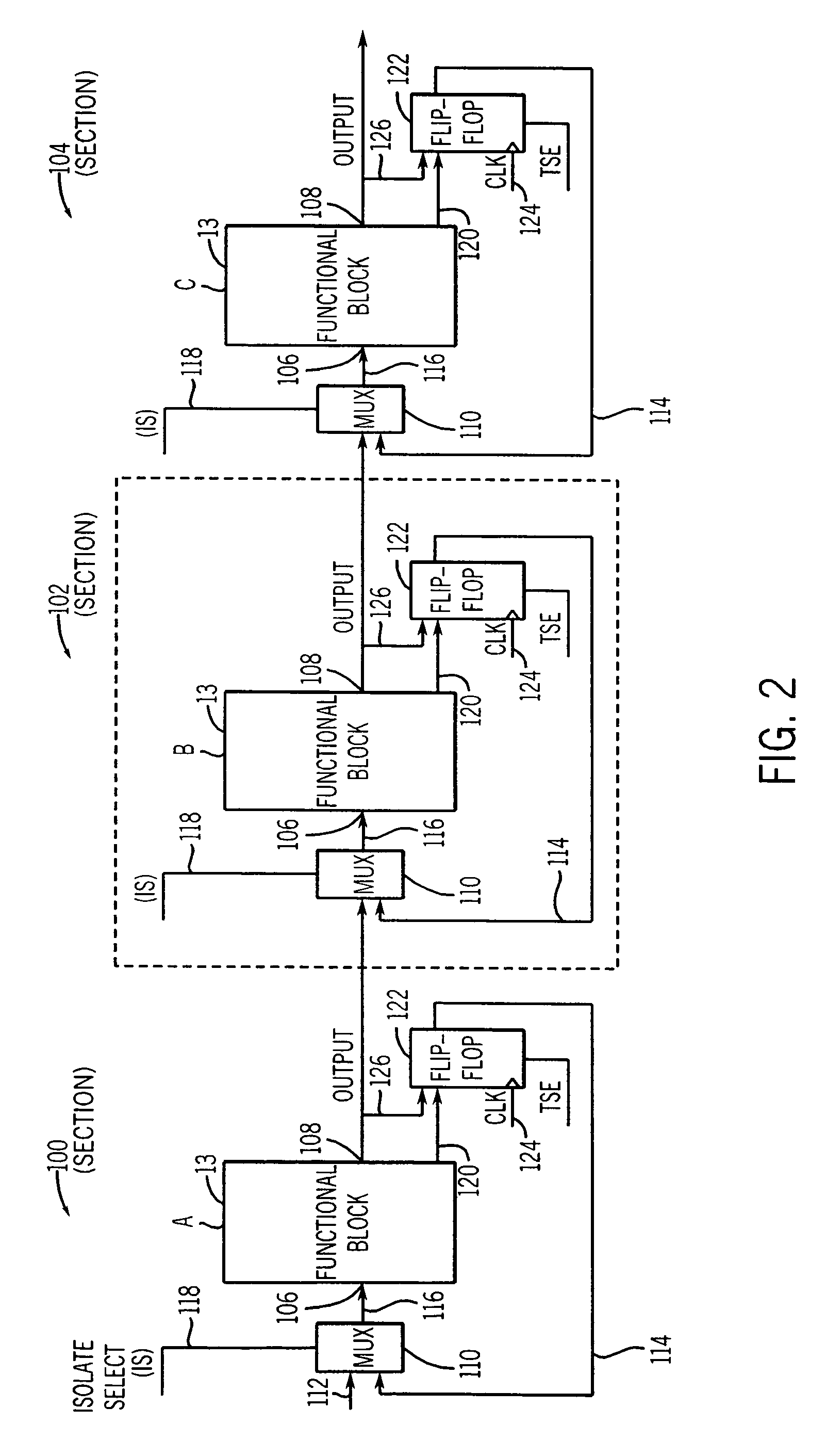
[0019]Referring to FIG. 2, an example of a series of functional blocks in accordance with the present invention is illustrated. Although three sections identified generally by sections 100, 102 and 104 are shown, such sections will be repeated along the integrated circuit and would be repeated in a chain or array. The number of sections is limited only by the number of functionalities in the integrated circuit. Each section 100, 102 and 104 includes a functional block A, B and C, respectively. Each functional block A, B and C is a section of logic that performs a function that is able to be partitioned from the remainder of the integrated circuit. Functional blocks A, B and C may in themselves be complex circuits that together form a single function.

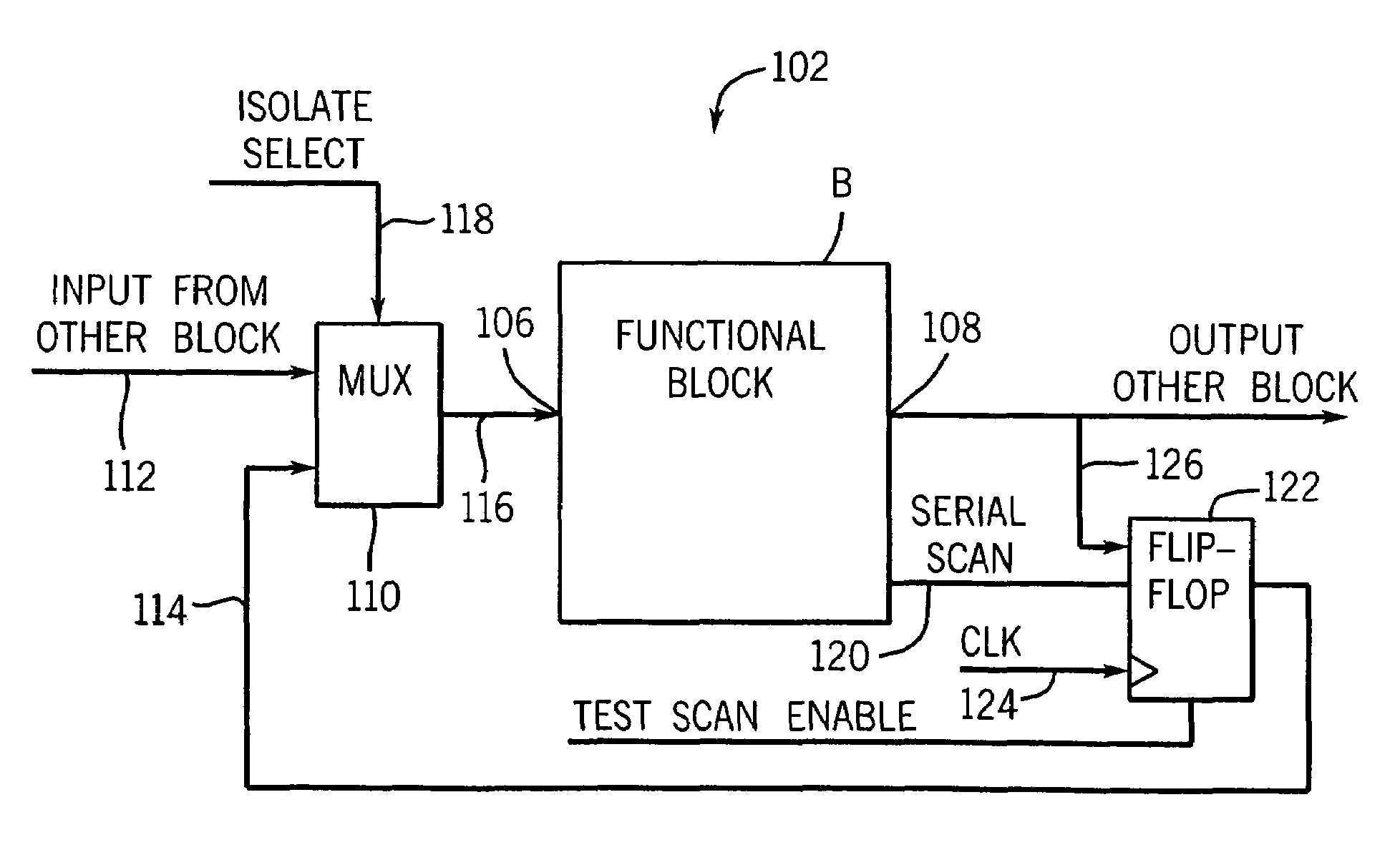
[0020]Referring to FIG. 3, section 102 of FIG. 2 is shown. It is to be understood that the functions, electrical connections and relationships between the functional block and the testing logic are the same for sections 100 and 104, as w...


PUM


Abstract

A method and system for partial scan testing of integrated circuits is disclosed. The invention includes determining at least one failed functional block during testing of the integrated circuit. The failed functional block is then logically isolated from the remaining non-failing functional blocks. Scan testing of the remainder of the non-failing functional blocks then occurs to determine the integrity of the remainder of the integrated circuit. The data coming out of the failing functional block is not allowed into the other functional blocks as input data. The invention allows the integrated circuit to be used and sold at a reduced functionality for applications not requiring the failed functional block(s).

Description

[0001]This application is a division of application Ser. No. 09 / 651,456, filed Aug. 30, 2000, now U.S. Pat. No. 6,515,483.BACKGROUND OF THE INVENTION[0002]The present invention relates generally to the testing of integrated circuits. More particularly, the invention relates to scan testing of integrated circuits to determine failed functional blocks and partially scan testing the integrated circuit without the failed functional blocks such that the integrated circuit may be tested and sold at a reduced functionality.[0003]Integrated circuitry on a chip is commonly tested. Scan testing is a common way to test integrated circuits by serially shifting test data into an integrated circuit, and then observing the output of the serial data. This method is very effective to determine whether an entire integrated circuit is functioning properly, and may be packaged and sold. The production chips of an integrated circuit to be sold are checked for manufacturing flaws before being furnished t...

Claims


Application Information

Patent Timeline
Patent Type & Authority Patents(United States)
IPC IPC(8): G01R31/28G01R31/3185
CPCG01R31/318558
Inventor PORTERFIELD, A. KENT
Owner MICRON TECH INC
Why Eureka
Try Eureka