Device for registration of optical holograms on the amorphous molecular semiconductor films

a technology of amorphous molecular semiconductor and optical hologram, which is applied in the field of optical hologram registration on the amorphous molecular semiconductor films, can solve the problems of destroying the registering medium, unable to achieve the maximum achievable and reproducible band parameters of the spatial frequency of the transmitting, and unable to register holograms, etc., to achieve the effect of reducing the dark conductivity of the ams-film and eliminating bulk and surface space charges

Inactive Publication Date: 2006-02-14
AGELLIS GROUP
View PDF15 Cites 1 Cited by
  • Summary
  • Abstract
  • Description
  • Claims
  • Application Information

AI Technical Summary

Benefits of technology

[0033]It is also an object of the invention to provide a device for registration of optical holograms that allows setting of an optimal initial temperature of the AMS-film, achieves the maximum surface potential during charging of the AMS-film prior to registration of the holographic image, reduces the dark conductivity of the AMS-film to a minimum, is able to create long lived latent images, eliminates the bulk and surface space charges of the AMS-film prior to erasing the developed image, restricts the development and erasing process by the pre-set value of the diffraction efficiency as measured in the zeroth order of diffraction, provides automatic determination of exposure times, and that is suitable for universal use and which is independent upon the optical scheme employed.

Problems solved by technology

The mean temperature of the registering medium progressively increases at its continuous cyclic operation and it may reach a value at which the hologram registration would be impossible and the destruction of the registering medium might occur.
However, despite allowing restriction of the development and erasing processes by the fundamental parameter, namely the diffraction efficiency, and the termination of cyclic operation of the device when the mean temperature of the AMS-film reaches the pre-set value, this device has a number of essential drawbacks:
It does not allow the maximum achievable and reproducible band parameters for spatial frequencies of the transmitting characteristics, the optimal spatial frequency of the transmitting characteristics, the resolution, holographic sensitivity, and the “signal-to-noise” ratio in the restored holographic image, which are determined by the heating rate of the AMS-film during the development of the latent electrostatic image.
It does not allow to obtain the optimal surface potential at which the local breakdowns of the AMS-film have yet not occurred, as well as the optimal charging current of the corona discharge at which the AMS-film surface is not damaged under ion deposition.
Thus, it does not allow to reach the maximum achievable and reproducible values of the signal-to-noise ratio in the restored holographic image, the ratio of reference-object beam intensities at hologram registration, the spatial frequency band of transmitting characteristic, the optimal spatial frequency of transmitting characteristic, and the holographic sensitivity.
This is caused by the device's lack of control of the charging current of the corona discharge, and the measurement and restriction of the surface potential of AMS-film during its charging by the corona discharge.
It does not reach the maximum achievable band parameters for spatial frequencies of the transmitting characteristics, the optimal spatial frequency of the transmitting characteristics, the holographic sensitivity, and the “signal-to-noise” ratio that are partly being determined by the relaxation rate of the latent electrostatic image prior to and during the development process, since the device does not provide reduction of the dark conductivity.
It can not be employed for double-exposure holographic interferometry when the delay time after registration of the first hologram exceeds 1 min, since the device does not provide the formation of a long-lived latent image having large relaxation times.
It does not allow preservation of the high “signal-to-noise” ratios, the band of spatial frequencies of the transmitting characteristics, the optimal spatial frequency of the transmitting characteristics, the holographic sensitivity under the repeated registrations, and the development and erasing of holograms that are determined in part by the time and temperature of erasing of the developed image, since the device does not provide the elimination of the surface- and bulk space charges of the AMS-film prior to the erasing of the developed image.
Thus, the device is not a universal device that is independent on the optical scheme of hologram registration.
Besides, the device does not provide termination of the hologram developing process in the case when the diffraction efficiency for some reason cannot reach the pre-set value.
The latter circumstance can lead to overheating the AMS-film and its failure.
The device does not provide the automatic determination of exposure time and consequently, automatic setting of the operation time for the expose time-relay.
Manual determination of the expose time and the adjustment of the expose time-relay reduce the operation efficiency of the device.

Method used


Image

  • Device for registration of optical holograms on the amorphous molecular semiconductor films
  • Device for registration of optical holograms on the amorphous molecular semiconductor films

Examples


Embodiment Construction

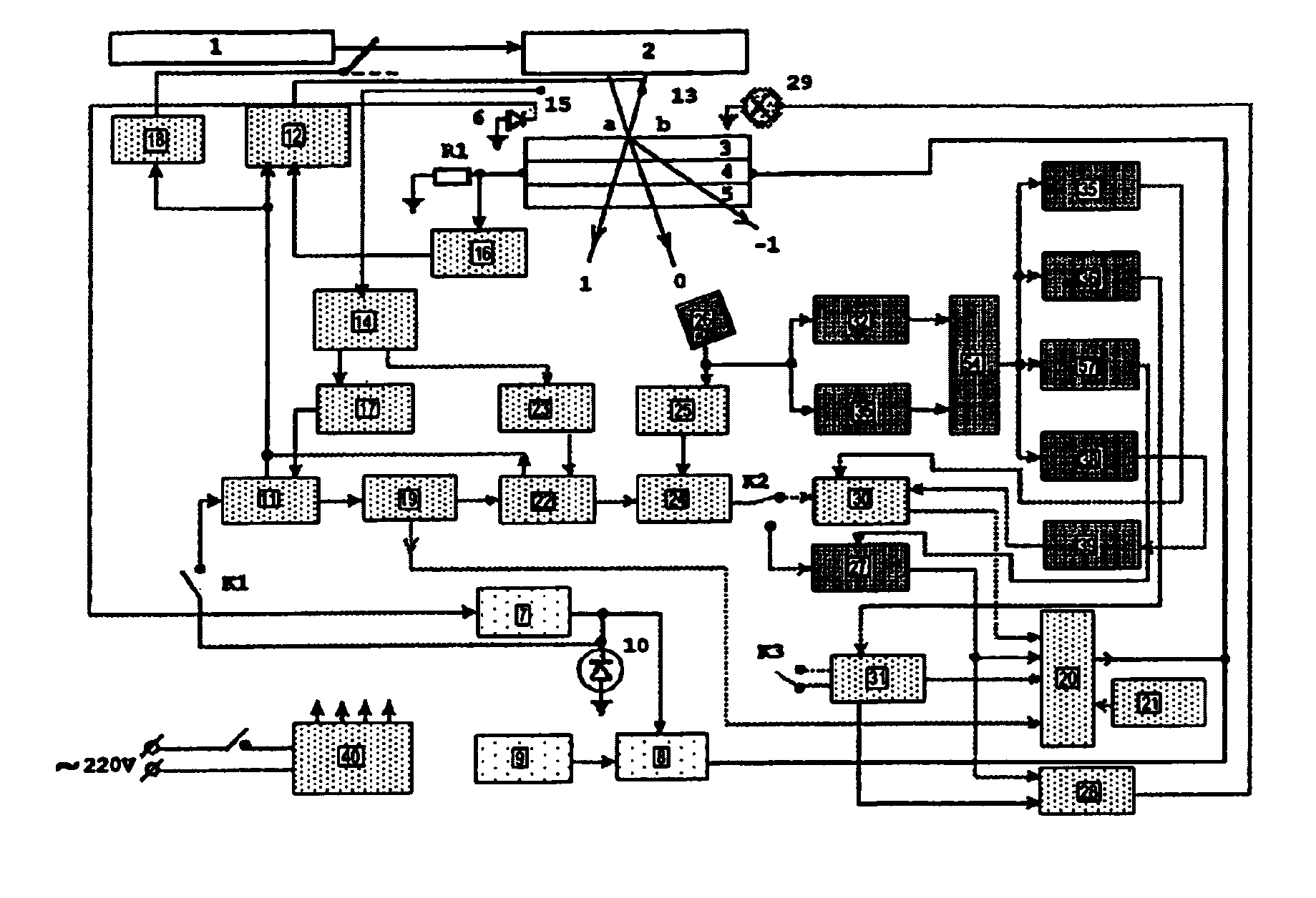
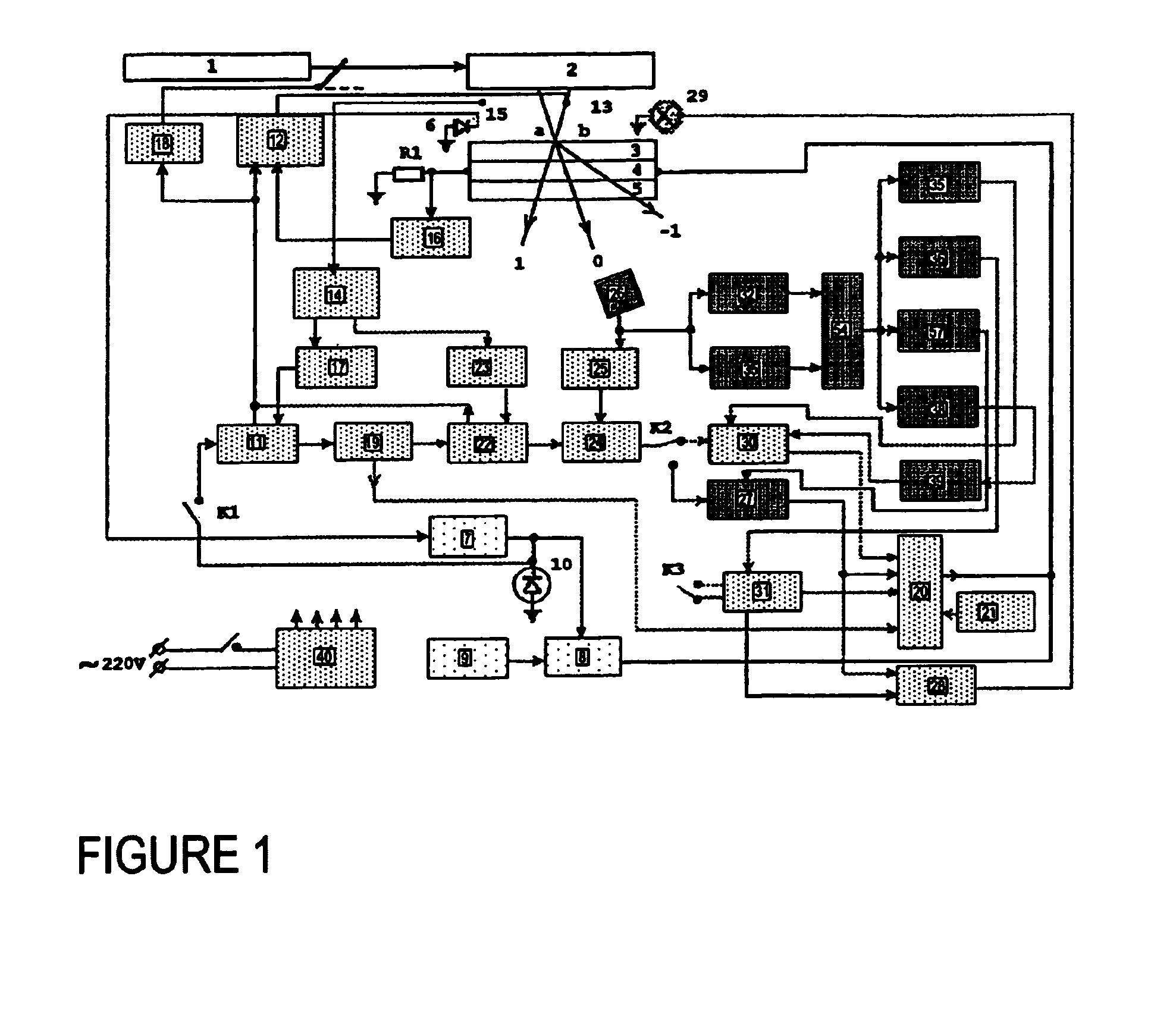
[0046]The invention will now be described in greater detail by reference to the block-diagram presented in FIG. 1 which show a control device for registering optical holograms according to a preferred embodiment of the invention. The control device consists of:[0047]A source 1 of coherent light (laser) with an optical scheme 2 of hologram formation,[0048]a registering medium 3–5, where 3 is the AMS-film containing 92 wt % of a copolymer comprising N-epoxypropylcarbazole copolymer with 5 wt % buthy1glycedile ether doped with 5 wt % methyl-9-(4-dodecyl-oxyphenyl-1,3-selenathiol-2-ylidene)-2,5,7-trinitrofluorene-4-carboxylate (MDOSTFC) and 4 wt % hexadecyl-2,7-dinitro-dicyanomethylenfluorene-4-carboxylate (HDDFC),[0049]an electric circuit 6–10 for the setting of the optimal initial temperature of the registering medium, where 6 is a temperature sensor installed immediately on the AMS-film surface 3, 7 is an initial temperature comparator which sets the initial temperature, compares the...


PUM


Abstract

This invention relates to the field of holography, in particular to a method and a device for recording optical holograms by means of amorphous molecular semiconductor (AMS) films deposited on a glass substrate pre-covered with a transparent electric conducting sub-layer. More precisely, the invention relates to a method and device for registering optical holograms on AMS-films which operates in such a way that the AMS-films possess the maximum achievable information parameters: Holographic sensitivity, optimal spatial frequency of the transmitted characteristic, band parameters for the spatial frequencies of the transmitted characteristic, “signal-to-noise” ratio in the restored holographic image, reference and object beam intensities ratio during hologram registration, and cycling ability. It is also an advantage that the device provides optimal operation efficiency of the registering media based on AMS-films, and restricts the development and erasing of the hologram upon reaching the pre-set value of the diffraction efficiency measured in the zeroth order of diffraction. The latter makes the device a universal device.

Description

[0001]This application is a divisional of co-pending application Ser. No. 09 / 596,556, filed on Jun. 19, 2000, the entire contents of which are hereby incorporated by reference and for which priority is claimed under 35 U.S.C. § 120; and this application claims priority of Application No. 2000 2948 filed in Norway on Jun. 8, 2000 under 35 U.S.C. § 119.[0002]This invention relates to the field of holography, in particular to a method and a device for recording optical holograms by means of amorphous molecular semiconductor (AMS) films deposited on a glass substrate.BACKGROUND[0003]A particular suited media for recording optical holograms are amorphous molecular semiconductor films. In this invention it is preferred to employ an AMS-film deposited on a glass substrate pre-covered with a conducting sub-layer, where the AMS-film consists of 92 wt % of a copolymer comprising N-epoxypropylcarbazole and 5 wt % buthylglycedil ether, doped with 5 wt % of methyl-9-(4-dodecyl-oxyphenyl-1,3-sele...

Claims


Application Information

Patent Timeline
Patent Type & Authority Patents(United States)
IPC IPC(8): G03H1/02G01B11/16
CPCG01B11/164G03H1/02G03H2001/0268G03H2260/53G03H2001/0264
Inventor FJELDSTAD, JOHN PETTERFJELDSTAD, IRINA EVGENIEVNALOBANOV, LEONID MIKHAILOVICHPIVTORAK, VJACHESLAV AVTONOMOVICHKUVSHINSKY, NIKOLAY GEORGIEVICHKOSTENKO, LEONID IVANOVICHKADASHCHUK, ANDREY KONSTANTINOVICHKUSHNIRUK, VLADIMIR PETROVICHPAVLOV, VALERIY ALEKSANDROVICH
Owner AGELLIS GROUP
Why Eureka
Try Eureka