Power assisted automatic supervised classifier creation tool for semiconductor defects

a technology of automatic supervision and classifier, applied in the field of software programs, can solve the problems of increasing production cost, affecting yield, and taking many hours

Inactive Publication Date: 2006-02-14
KLA TENCOR TECH CORP
View PDF18 Cites 125 Cited by
  • Summary
  • Abstract
  • Description
  • Claims
  • Application Information

AI Technical Summary

Benefits of technology

[0019](iii) Dynamic Classifier Controls and Performance Tools: This allows the user to visualize and optimize the parameters of the classifier even further. As in (ii), the resulting performance is immediately visible.
[0020](iv) Unsupervised Automatic Classifier

Problems solved by technology

As new materials, methods, and processes are introduced into semiconductor manufacturing, new defects are emerging in the manufacturing process that can great

Method used


Image

  • Power assisted automatic supervised classifier creation tool for semiconductor defects
  • Power assisted automatic supervised classifier creation tool for semiconductor defects
  • Power assisted automatic supervised classifier creation tool for semiconductor defects

Examples


Embodiment Construction

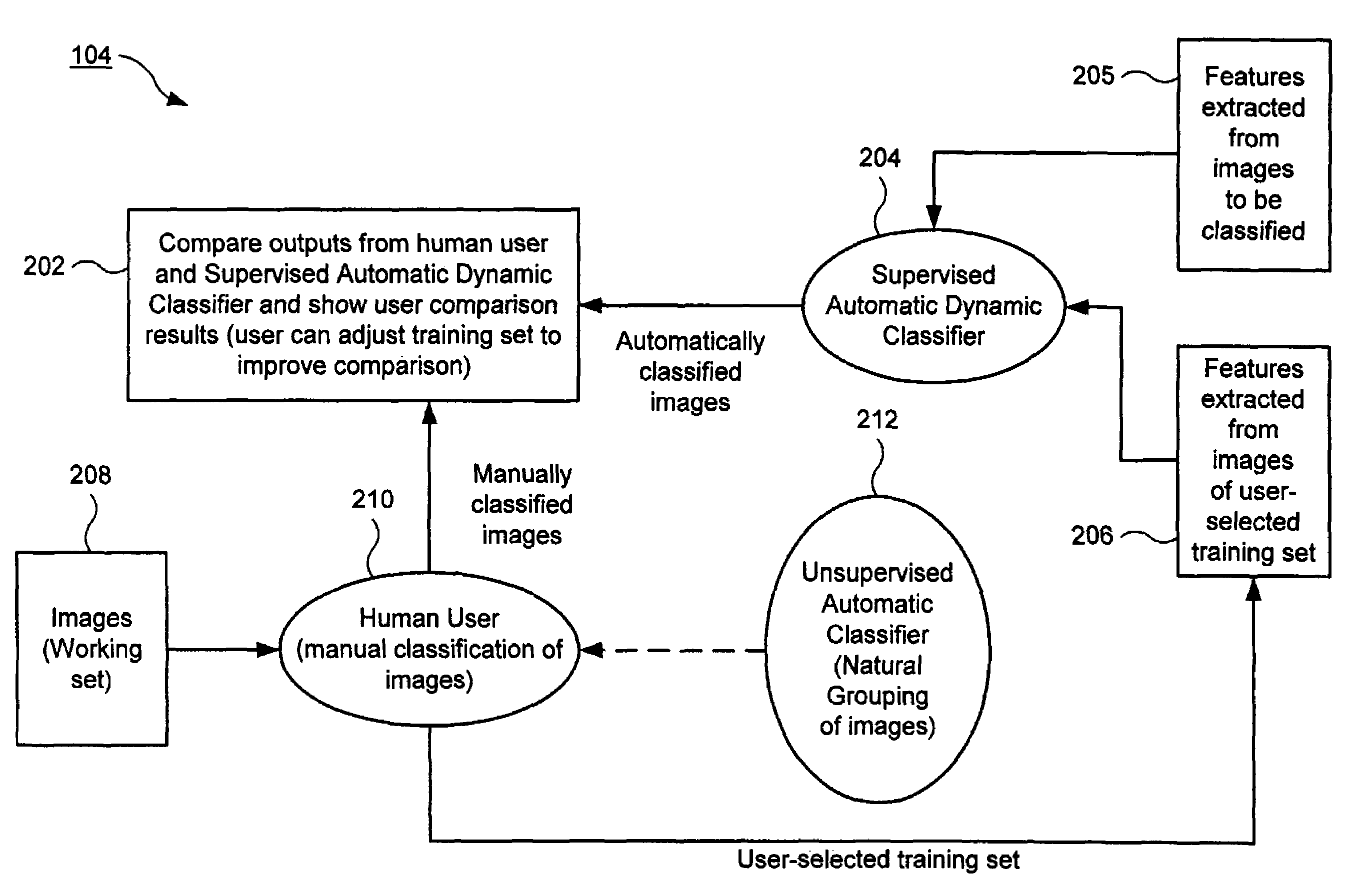
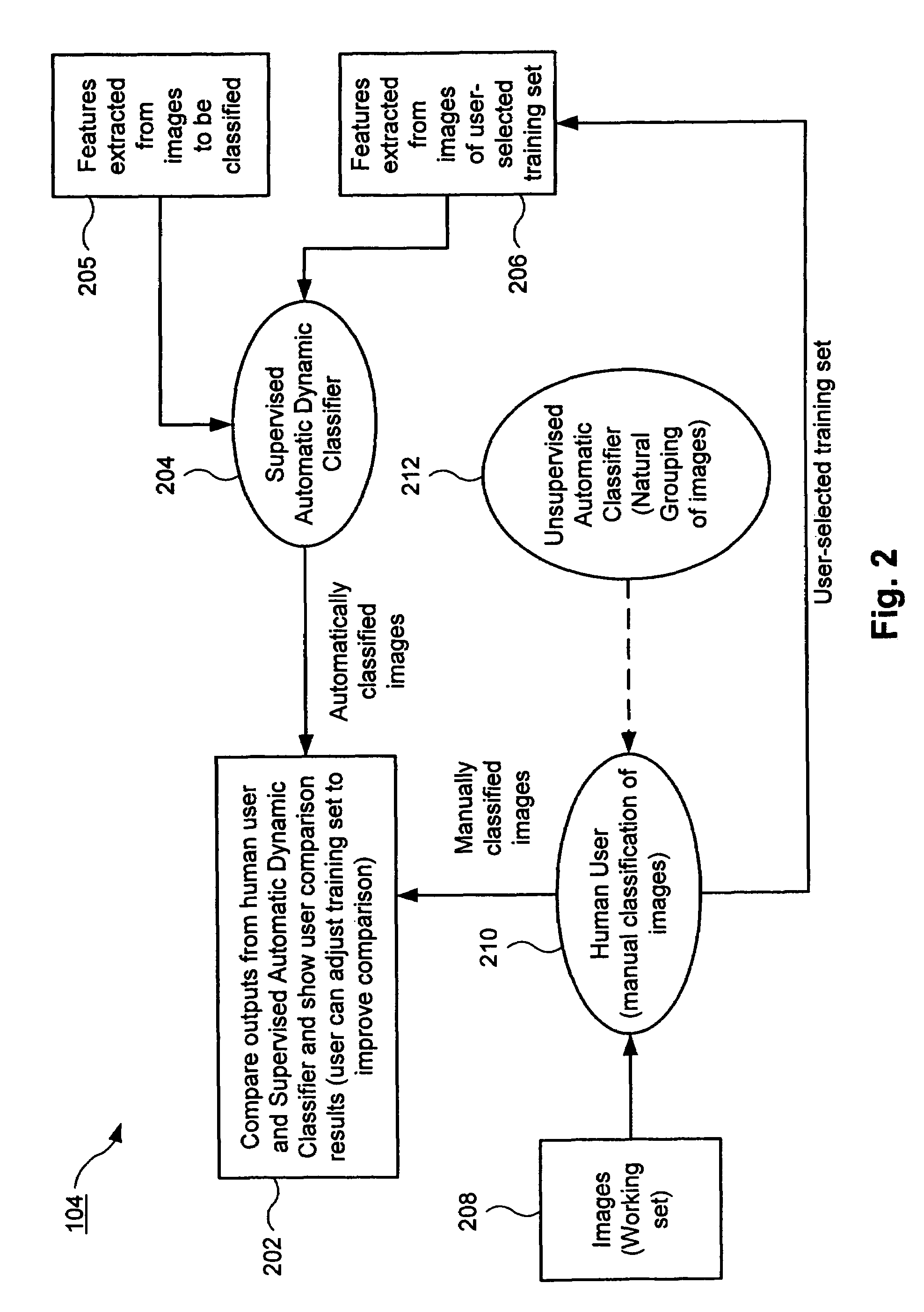
[0034]The described embodiments of the present invention aid a user in classifying defect images input to the system from an outside source. For example, the images can be received from a scanning electron microscope (SEM), a defect inspection system, such as KLA-Tencor's 2132 inspection tool, or any similar instrument used to generate images and detect errors therein. In certain embodiments, the images can come from more than one type of input source. For example, images may be received from both an SEM and a 2132 inspection tool. Different types of images received from different sources can aid in defect classification, since different types of images produce more information is provided concerning the defects to be classified. The images also can be point locations on wafers.

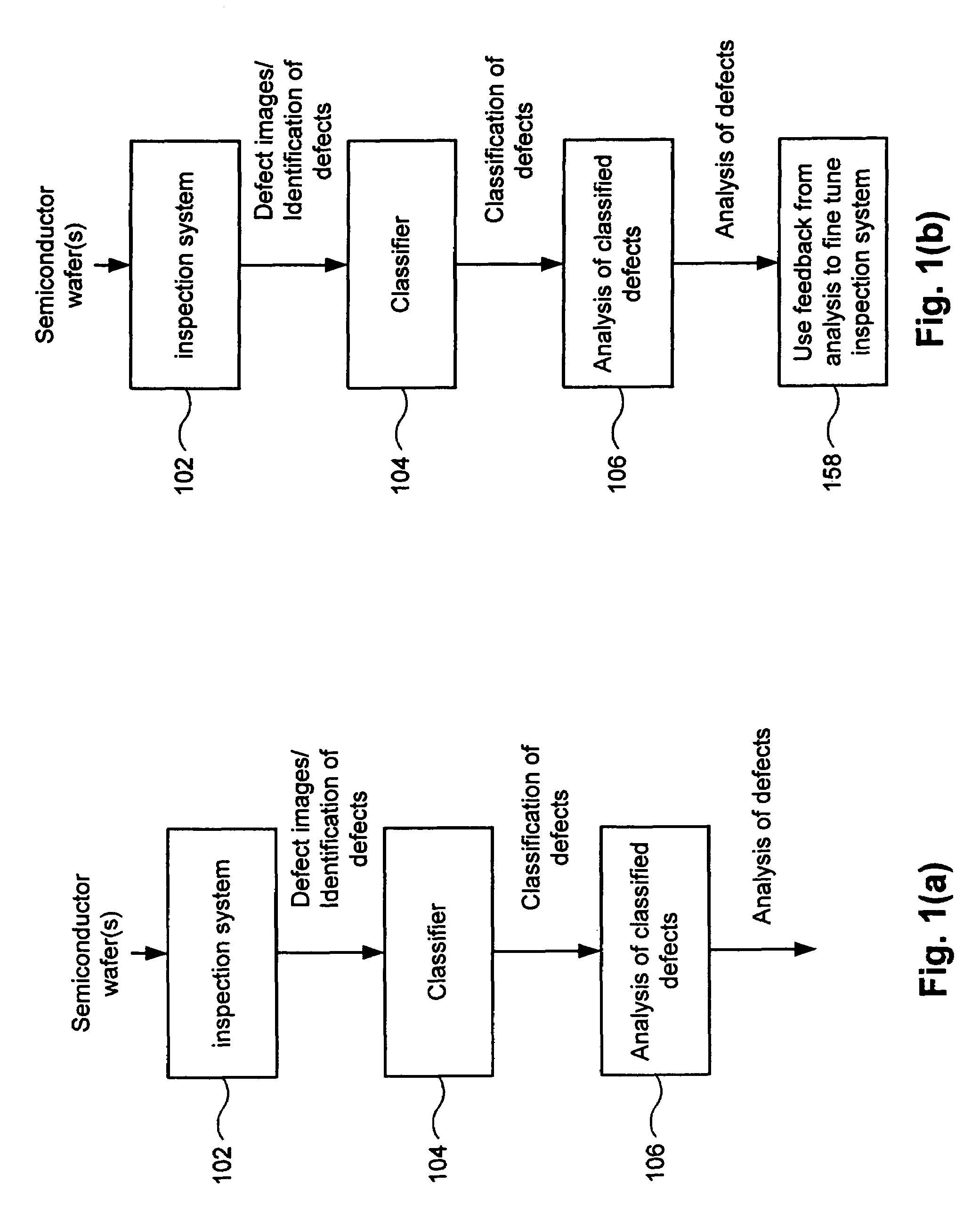
[0035]FIG. 1(a) is a block diagram showing an overview of a semiconductor optical, ebeam, or other types of inspection systems. As discussed above, defect images are preferably received from an outside source...


PUM


Abstract

A method and system that optionally allows a user to view image defects organized by natural groupings based on features of the images. The natural groupings make it easier for the user to organize some or all of the images into classes in a training set of images. A feature vector is extracted from each image in the training set and stored, along with its user-specified class, for use by an automatic classifier software module. The automatic classifier uses the stored feature vectors and classes to automatically classify images not in the training set. If the automatically classified images do not match images manually classified by the user, the user modifies the training set until a better result is obtained from the automatic classifier. The system can provide feedback to an inspection system designed to aid in the setup and fine-tuning of the inspection system.

Description

RELATED APPLICATIONS[0001]This application claims priority under 35 U.S.C. § 119(e) to U.S. Provisional Application Ser. No. 60 / 167,955 entitled “power Assisted Automatic Supervised Classifier Creation Tool for Semiconductor Defects,” of Bakker, Banerjee, and Smith et al., filed Nov. 29, 1999.[0002]The following applications are related to this application and are herein incorporated by reference:[0003]1. U.S. application Ser. No. 08 / 958,288 of Hardikar et al., filed Oct. 27, 1997.[0004]2. U.S. application Ser. No. 08 / 958,780 of Hardikar et al., filed Oct. 27, 1997.[0005]The following U.S. patent is related to this application and is herein incorporated by reference:[0006]1. U.S. Pat. No. 5,226,118 to Baker et al., issued Jul. 6, 1993.BACKGROUND OF THE INVENTION[0007]1. Field of the Invention[0008]The present invention relates generally to software programs and, more generally, to software-controlled optical, ebeam, or other types of inspection systems for semiconductor wafers.[0009...

Claims


Application Information

Patent Timeline
IPC IPC(8): G06K9/62G06T5/00H01L21/66
CPCG06T7/0004G06T2207/10056G06T2207/30148G06T2207/20092G06T2207/20081
Inventor BAKKER, DAVIDBANERJEE, SAIBALSMITH, IAN R.
Owner KLA TENCOR TECH CORP
Why Eureka
Try Eureka