Wafer and method of producing a substrate by transfer of a layer that includes foreign species

a technology of transfer layer and substrate, which is applied in the direction of basic electric elements, semiconductor devices, electrical equipment, etc., can solve the problems of large production cost, difficult production of large inp crystals, and heterostructures that cannot be obtained by epitaxy alone, so as to achieve greater uniformity and controllability.

Active Publication Date: 2006-03-07
S O I TEC SILICON ON INSULATOR THECHNOLOGIES +1
View PDF5 Cites 32 Cited by
  • Summary
  • Abstract
  • Description
  • Claims
  • Application Information

AI Technical Summary

Benefits of technology

The present invention allows for better control over the amount of a certain substance that has been added during production. This helps create more consistent results across different parts of the product. Additionally, it doesn't negatively impact any other steps involved in the process.

Problems solved by technology

The technical problem addressed in this patent is how to improve the process of forming semiconductor devices without reducing the formation of defects caused by the traditional methods of carrying out heat treatment when manufacturing integrated circuits. One solution involves the use of a method called smart-cut™, where a thin layer of material is removed from a host substrate through laser ablation. However, there are challenges involved in integrating different materials together due to differences in their respective crystallization properties. Additionally, issues related to the absence of suitable substrates often result in shortages of resources and increases in laboratory space utilization rates.

Method used


Image

  • Wafer and method of producing a substrate by transfer of a layer that includes foreign species
  • Wafer and method of producing a substrate by transfer of a layer that includes foreign species
  • Wafer and method of producing a substrate by transfer of a layer that includes foreign species

Examples


Embodiment Construction

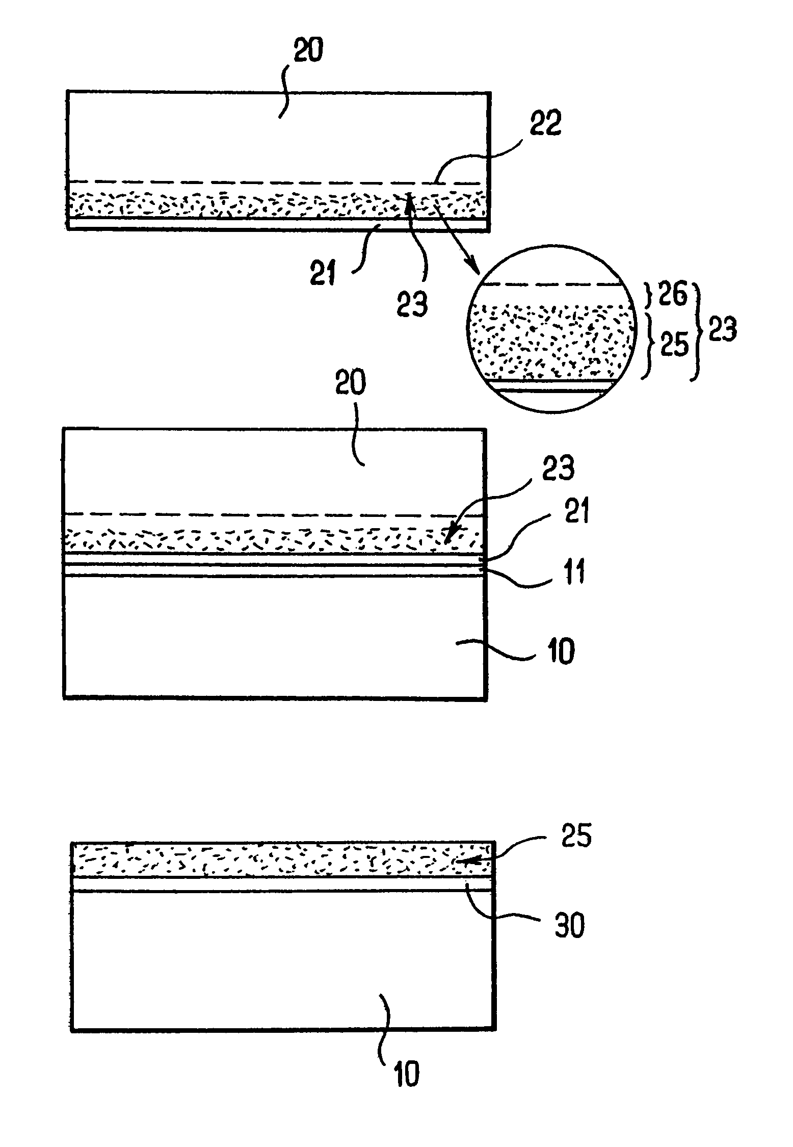
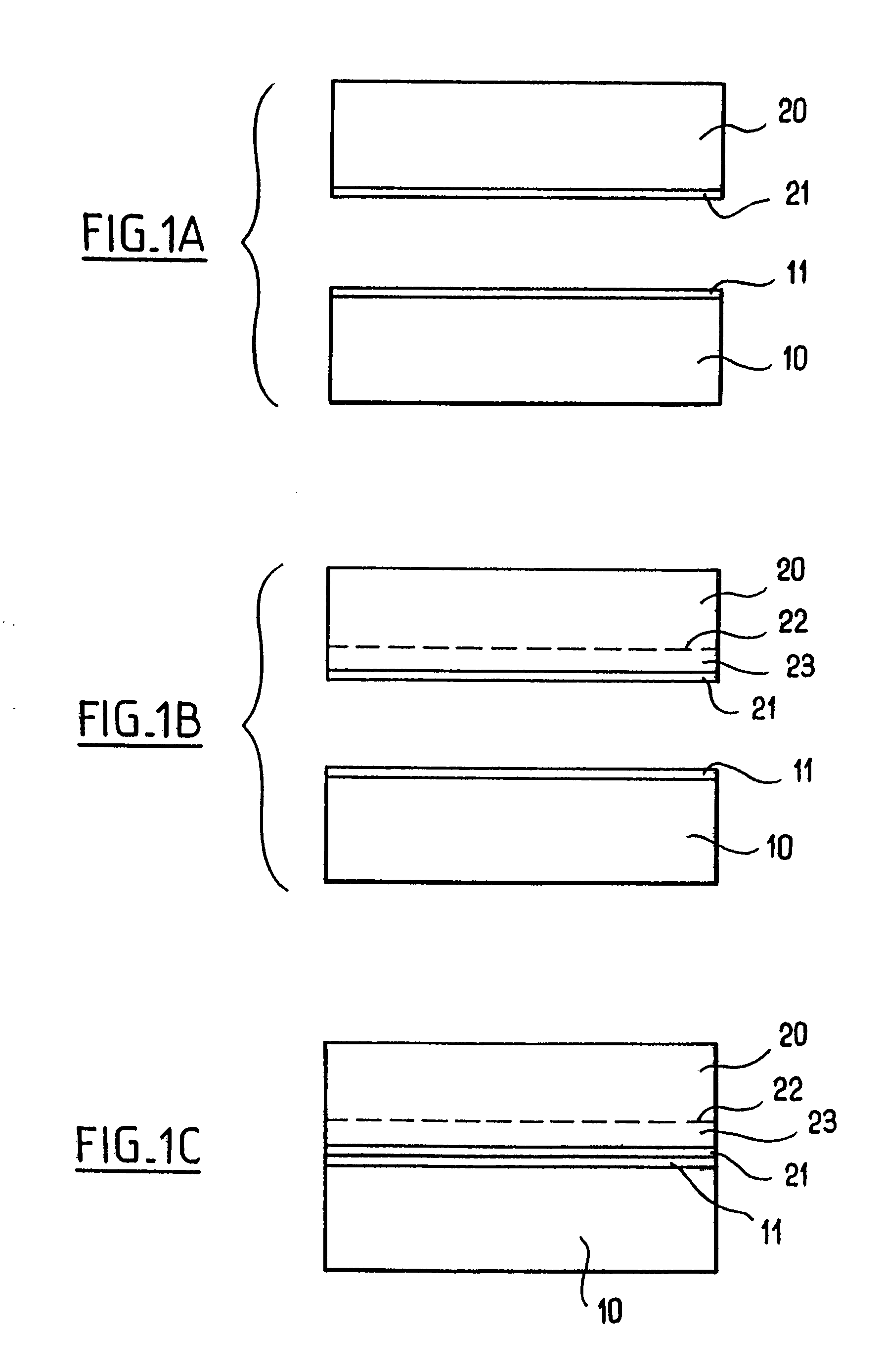
[0029]Although studies have demonstrated the favorable role played by the presence of dopants or impurities in the material on the coalescence kinetics of implanted species prior to cleavage, the Applicant has discovered that iron acts differently, probably by modifying the migration kinetics of hydrogen during implantation then during annealing. This means that the selection of implantation conditions (dose, energy, temperature) and annealing conditions (duration, temperature) becomes much more difficult. Further, the roughness of the free face of the transferred layer following detaching is increased, thus increasing the polishing work and producing a material loss which harms the industrial efficiency and the economics of the method.

[0030]To overcome this, in a first aspect, the invention provides a method of producing a substrate comprising a transfer crystalline layer transferred from a donor wafer onto a support. The transfer layer includes one or more foreign species intended...


PUM


Abstract

A method of producing a substrate that has a transfer crystalline layer transferred from a donor wafer onto a support. The transfer layer can include one or more foreign species to modify its properties. In the preferred embodiment an atomic species is implanted into a zone of the donor wafer that is substantially free of foreign species to form an embrittlement or weakened zone below a bonding face thereof, with the weakened zone and the bonding face delimiting a transfer layer to be transferred. The donor wafer is preferably then bonded at the level of its bonding face to a support. Stresses are then preferably applied to produce a cleavage in the region of the weakened zone to obtain a substrate that includes the support and the transfer layer. Foreign species are preferably diffused into the thickness of the transfer layer prior to implantation or after cleavage to modify the properties of the transfer layer, preferably its electrical or optical properties. The preferred embodiment produces substrates with a thin InP layer rendered semi-insulating by iron diffusion.

Description


Claims


Application Information

Patent Timeline
Owner S O I TEC SILICON ON INSULATOR THECHNOLOGIES
Why Eureka
Try Eureka