
MEMS devices with unreleased thin film components

a technology of thin film components and mems devices, which is applied in the manufacture of interferometric modulators, instruments, non-linear optics, etc., can solve problems such as damage to the mems devi

Active Publication Date: 2006-03-14
SNAPTRACK
View PDF277 Cites 136 Cited by
  • Summary
  • Abstract
  • Description
  • Claims
  • Application Information

AI Technical Summary

Benefits of technology

[0003]One process for fabricating MEMS devices falls under the label of “surface micromachining” and comprises a sequence of deposition and etch steps that are repeated until a final step or release step. Such a process can often start with some kind of raw material in the form of films or thin film precursors which are deposited beforehand. These precursors may represent a definable component, which can be manufactured in high volumes in dedicated facilities. A more detailed description of this component is provided in patent application Ser. No. 10 / 606,001 herein incorporated by reference.

Problems solved by technology

During shipping of the MEMS device, movement of the mechanical structures can occur and may result in damage to the MEMS device.

Method used


Image

  • MEMS devices with unreleased thin film components
  • MEMS devices with unreleased thin film components
  • MEMS devices with unreleased thin film components

Examples


Embodiment Construction

[0011]In the following detailed description of embodiments of the invention, numerous specific details are set forth such as examples of specific materials, machines, and methods in order to provide a thorough understanding of the present invention. It will be apparent, however, to one skilled in the art that these specific details need not be employed to practice the present invention. In other instances, well known materials, machines, or methods have not been described in detail in order to avoid unnecessarily obscuring the present invention.

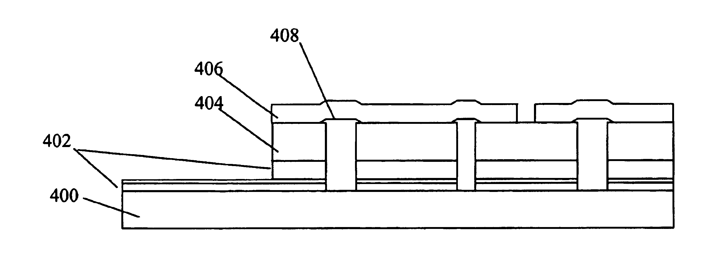
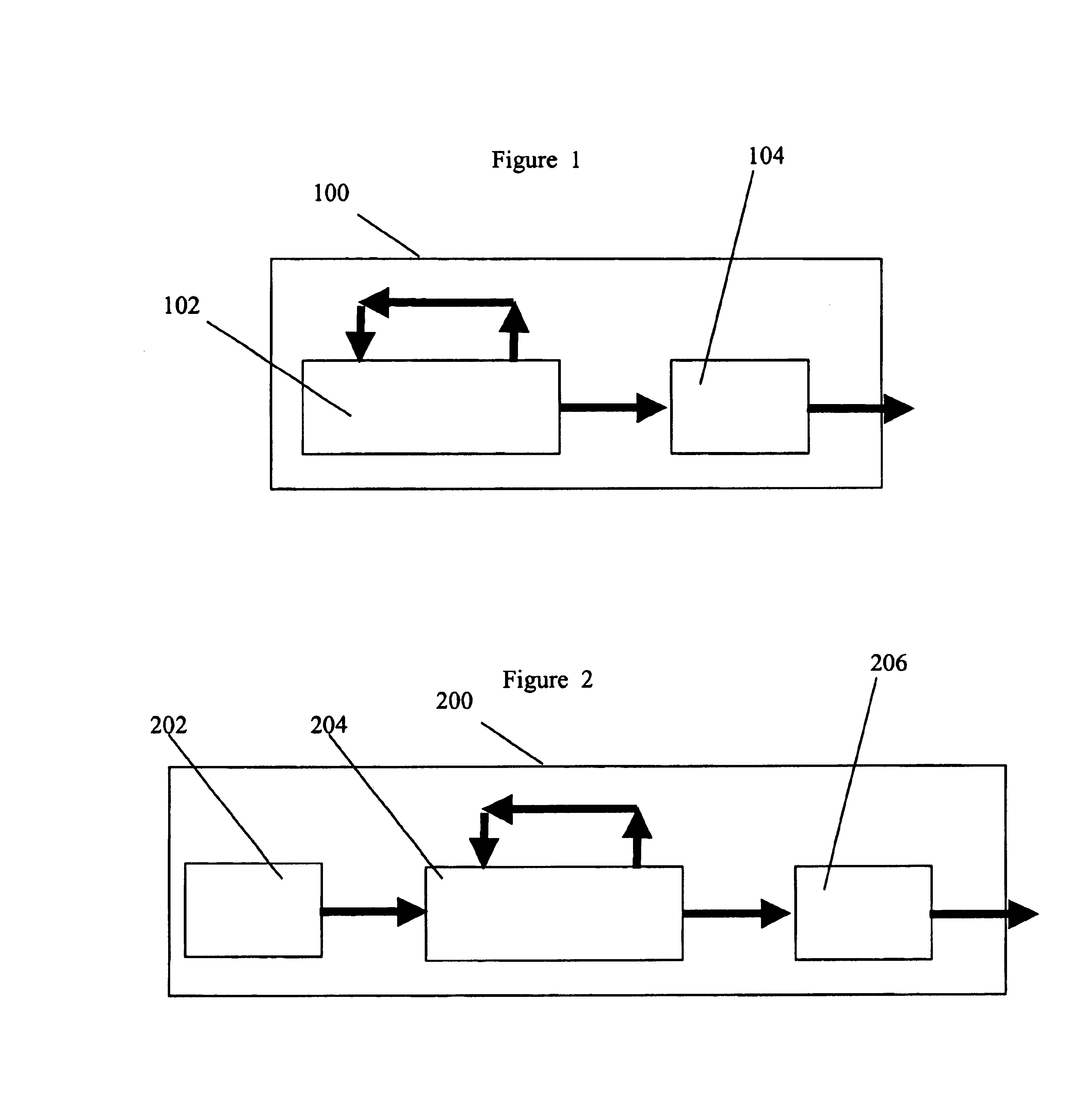
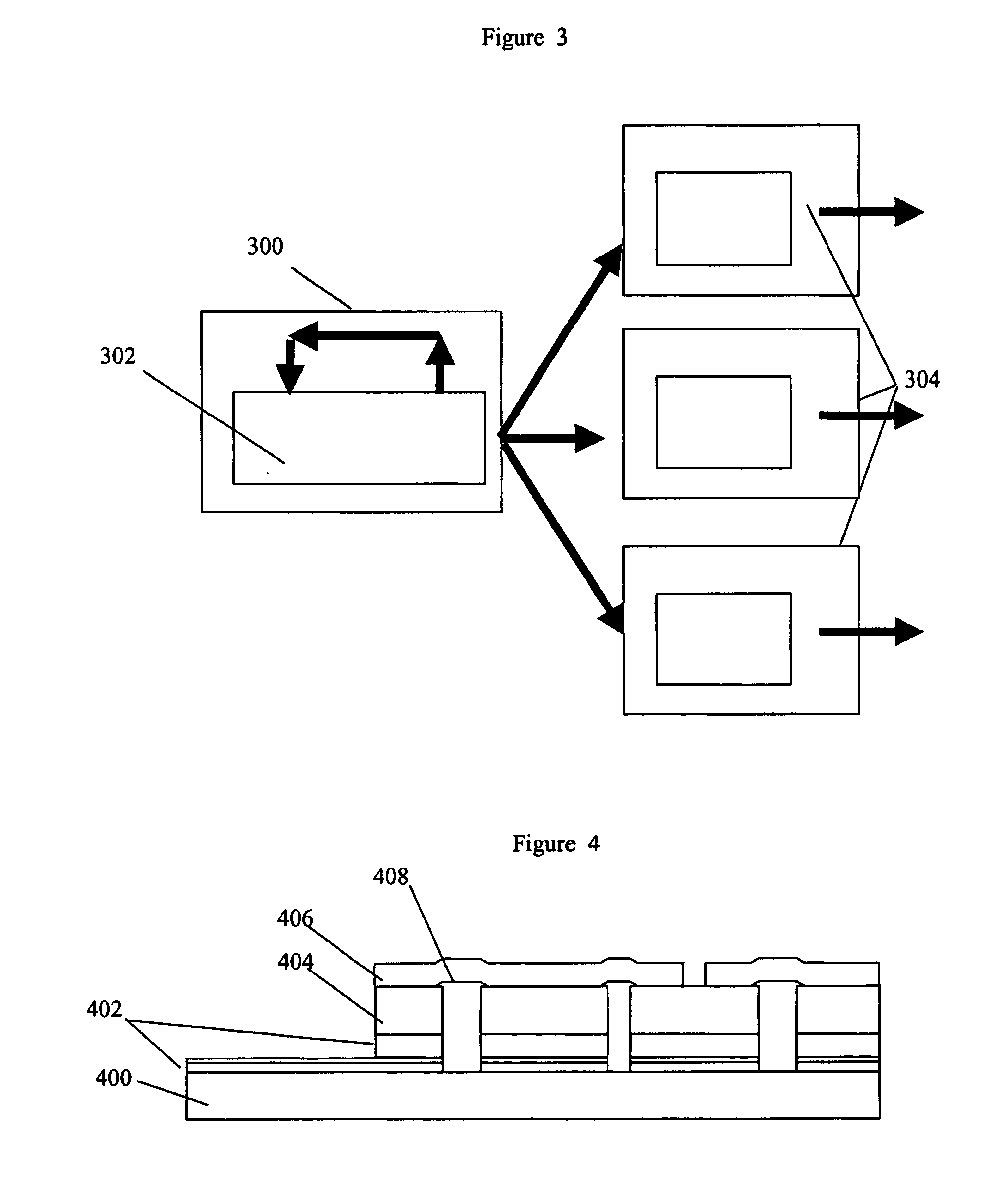
[0012]Broadly, in accordance with one embodiment of the invention, a MEMS device including a moveable component is fabricated, and the movement of the moveable component is inhibited using a sacrificial material, so that damage to the moveable component during shipping is at least reduced. In one embodiment, the sacrificial material is deposited during fabrication of the MEMS device, and the sacrificial material is removed during a release st...


PUM

PropertyMeasurementUnit
mechanicalaaaaaaaaaa
movementaaaaaaaaaa
volumesaaaaaaaaaa

Abstract

In one embodiment, the invention provides a MEMS device. The MEMS device comprises a plurality of functional components including at least one moveable component; and a sacrificial component to at least reduce movement of the moveable component during shipping of the microelectromechanical systems device, wherein the sacrificial component can be removed after shipping.

Description

FIELD OF THE INVENTION[0001]This invention relates generally to fabrication processes for microelectromechanical systems (MEMS) devices and more specifically to the manufacture of interferometric modulators (iMoDs).BACKGROUND OF THE INVENTION[0002]An interferometric modulator is a class of MEMS (microelectromechanical) systems devices which have been described and documented in a variety of patents including U.S. Pat. Nos. 5,835,255, 5,986,796, 6,040,937, 6,055,090, and U.S. Pending patent application Ser. Nos. 09 / 966,843, 09 / 974,544,10 / 082,397,10 / 084,893, and 10 / 078,282, herein incorporated by reference.[0003]One process for fabricating MEMS devices falls under the label of “surface micromachining” and comprises a sequence of deposition and etch steps that are repeated until a final step or release step. Such a process can often start with some kind of raw material in the form of films or thin film precursors which are deposited beforehand. These precursors may represent a definabl...

Claims


Application Information

Patent Timeline
Patent Type & Authority Patents(United States)
IPC IPC(8): G02B26/00H01L21/302B81B3/00B81C1/00
CPCB81C1/00896B81B3/00B81C1/00
Inventor MILES, MARK W.
Owner SNAPTRACK
Learn More