
Field-effect transistor with horizontal self-aligned gates and the production method therefor

Inactive Publication Date: 2006-04-04
COMMISSARIAT A LENERGIE ATOMIQUE ET AUX ENERGIES ALTERNATIVES
View PDF7 Cites 10 Cited by
  • Summary
  • Abstract
  • Description
  • Claims
  • Application Information

AI Technical Summary

Benefits of technology

[0012]Another aim still is to propose a transistor having reduced parasite capacities and improved dynamic behaviour.
[0034]According to yet another possibility, the lower gate can be delimited by self-aligned oxidation of the first gate layer. The effect of oxidation is to make the gate material locally insulating, and thus limit the lateral extension of the gate.
[0040]The interconnection of the gates allows the same potential for controlling the transistor to be applied to them, thus avoiding multiplying the gate access terminals.

Problems solved by technology

One of the main difficulties occurring in the manufacture of double-gate transistors is associated with alignment of the gates on one another, and with their alignment on the channel region.
The alignment of the gates is all the more delicate since miniaturisation of the transistors is considerable.
Another harmful effect of the dissymmetry of the transistors, particularly sensitive in numerical applications, is the approximate definition of the high and low (0 and 1) logic levels.

Method used


Image

  • Field-effect transistor with horizontal self-aligned gates and the production method therefor
  • Field-effect transistor with horizontal self-aligned gates and the production method therefor
  • Field-effect transistor with horizontal self-aligned gates and the production method therefor

Examples


Embodiment Construction

[0010]The aim of the present invention is to propose a double-gate transistor, which does not have the limitations specified hereinabove.

[0011]A goal in particular is to propose such a transistor, which is perfectly symmetrical for regular definition of high and low logic levels.

[0012]Another aim still is to propose a transistor having reduced parasite capacities and improved dynamic behaviour.

[0013]The final aim of the invention is to propose different processes for producing such a transistor.

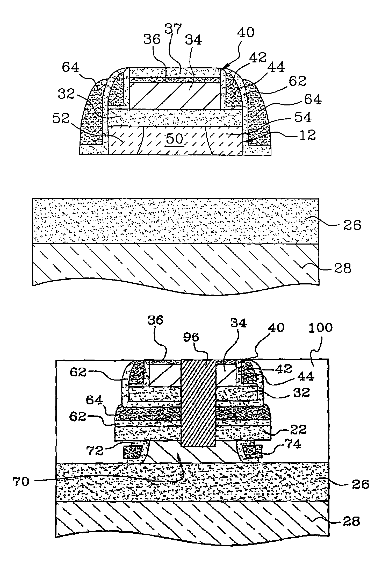
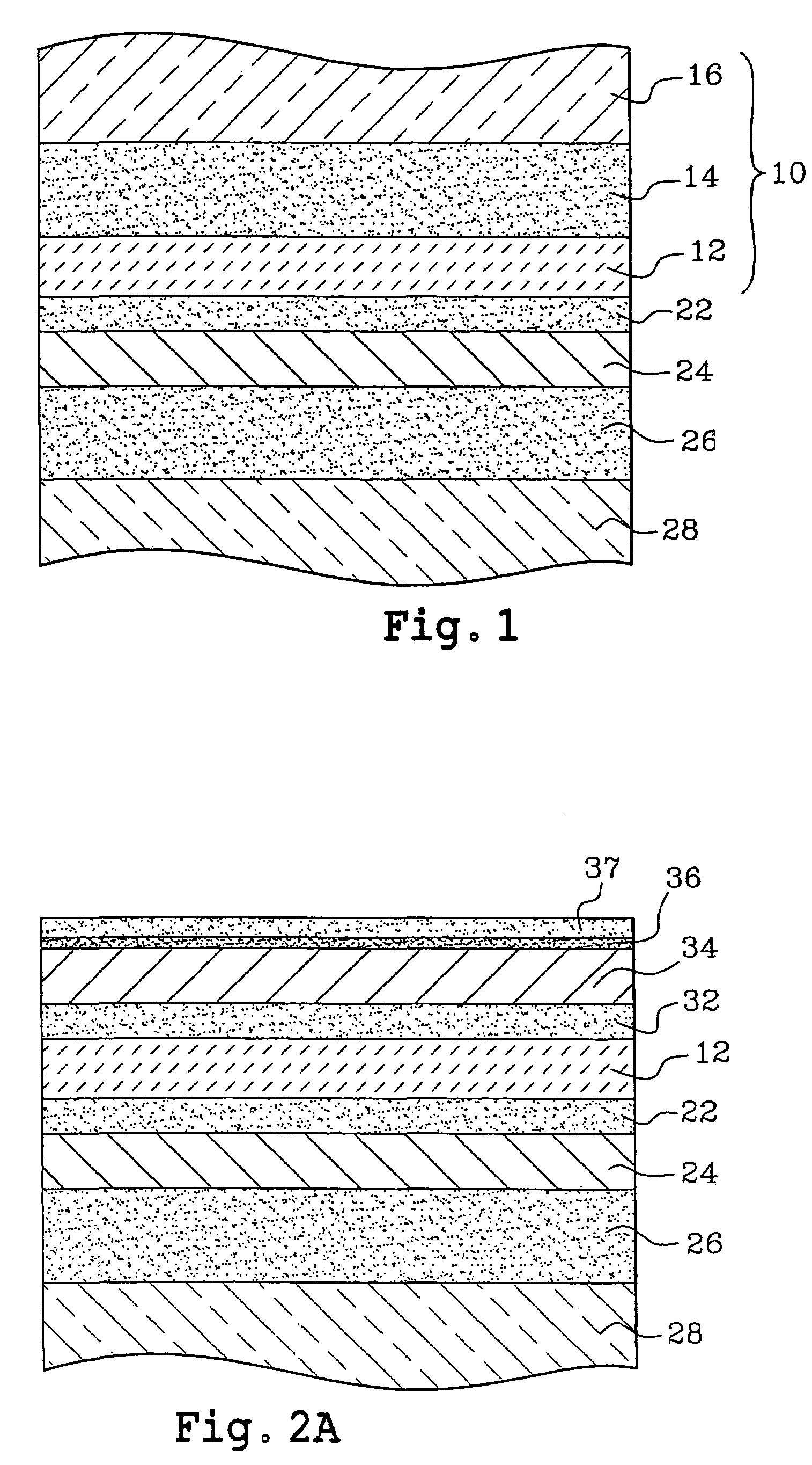
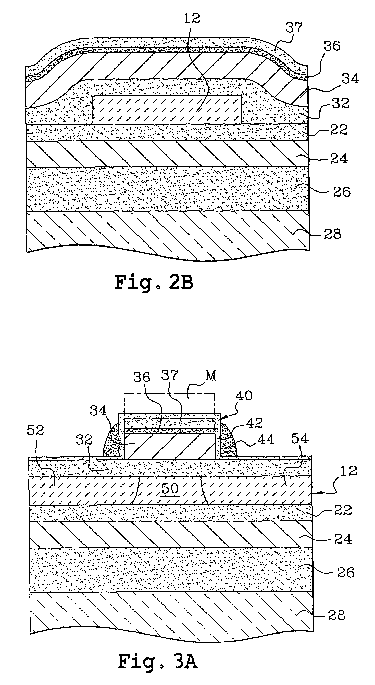
[0014]To achieve the aims specified hereinabove, the object of the invention more precisely is a field-effect transistor comprising on a substrate:[0015]an active region forming a channel,[0016]a first insulated gate associated with a first face of the active region,[0017]source and drain regions formed in a part of the active region, on either side of the channel, and self-aligned on the first gate,[0018]a second insulated gate associated with a second face of the active region, opposite the...


PUM


Abstract

A field-effect transistor including: a support substrate, an active area forming a channel; a first active gate which is associated with a first face of the active area; source and drain areas which are formed in the active area and which are self-aligned on the first gate; a second insulated gate which is associated with a second face of the active region opposite the first face of the active region. According to the invention, the second gate is self-aligned on the first gate and, together with the first gate, forms a mesa structure on a support substrate.

Description

TECHNICAL DOMAIN[0001]The present invention relates to a field-effect transistor, with horizontal self-aligned gates.[0002]It also relates to a process for manufacturing such a transistor.[0003]Transistor with horizontal gates is understood to mean a transistor whose gates extend substantially according to a plane parallel to a main face of a substrate on which the transistor is made. The invention relates in particular to a double-gate transistor, that is, a transistor comprising two gates placed on two opposite faces of a channel region.[0004]Transistors of the type mentioned hereinabove are used mainly in the manufacture of numerical circuits, for making logic commutators or analogue circuits, for example for radiofrequency devices. Applications can be also found in other domains of electronics.PRIOR ART[0005]Documents (1) to (4), whereof the references are specified at the end of the description concern transistors with double insulated gate. In particular they are transistors f...

Claims


Application Information

Patent Timeline
IPC IPC(8): H01L21/336H01L21/8234H01L29/786
CPCH01L29/66772H01L29/78648H01L29/78645
Inventor DELEONIBUS, SIMON
Owner COMMISSARIAT A LENERGIE ATOMIQUE ET AUX ENERGIES ALTERNATIVES
Learn More