Dynamically adjustable probe tips

a technology of dynamic adjustment and probe tip, which is applied in the direction of mechanical measurement arrangement, mechanical roughness/irregularity measurement, instruments, etc., can solve the problems of difficult positioning of more than one conventional cantilever/probe tip proximate an integrated circuit, and the hardware of conventional probes is not suitable for holding and positioning,

Active Publication Date: 2006-04-04
GLOBALFOUNDRIES US INC
View PDF14 Cites 128 Cited by
  • Summary
  • Abstract
  • Description
  • Claims
  • Application Information

AI Technical Summary

Problems solved by technology

Although conventional probe cantilevers are themselves relatively small devices, the conventional hardware to hold and position them is not.
Furthermore, relative to the sizes of probed structures on integrated circuits, conventional probe cantilevers may also be characterized as large indeed.
As a result, it is difficult to position more than one conventional cantilever/probe tip proximate an integrated circuit.
In circumstances where closely spaced structures require

Method used


Image

  • Dynamically adjustable probe tips
  • Dynamically adjustable probe tips
  • Dynamically adjustable probe tips

Examples


Embodiment Construction

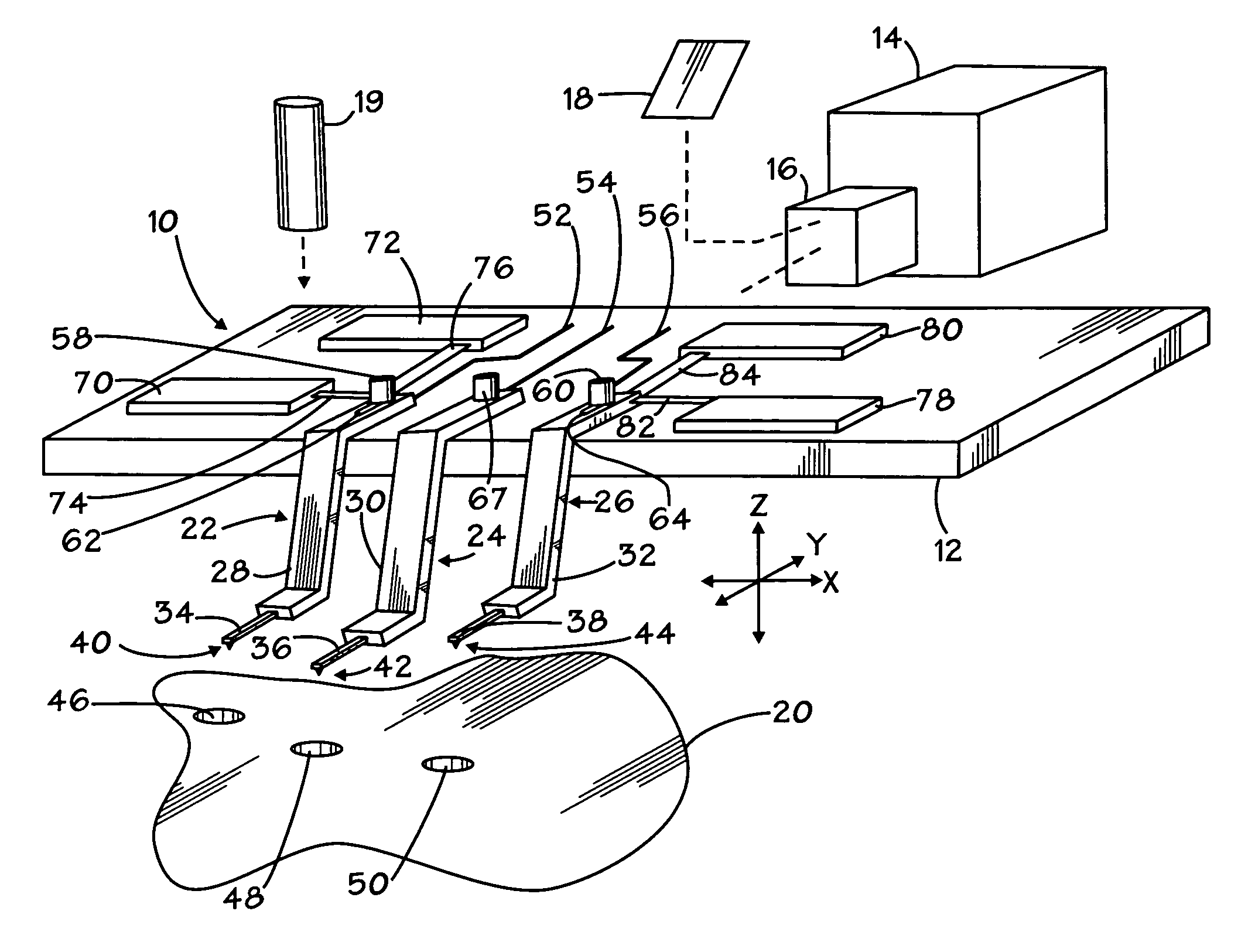
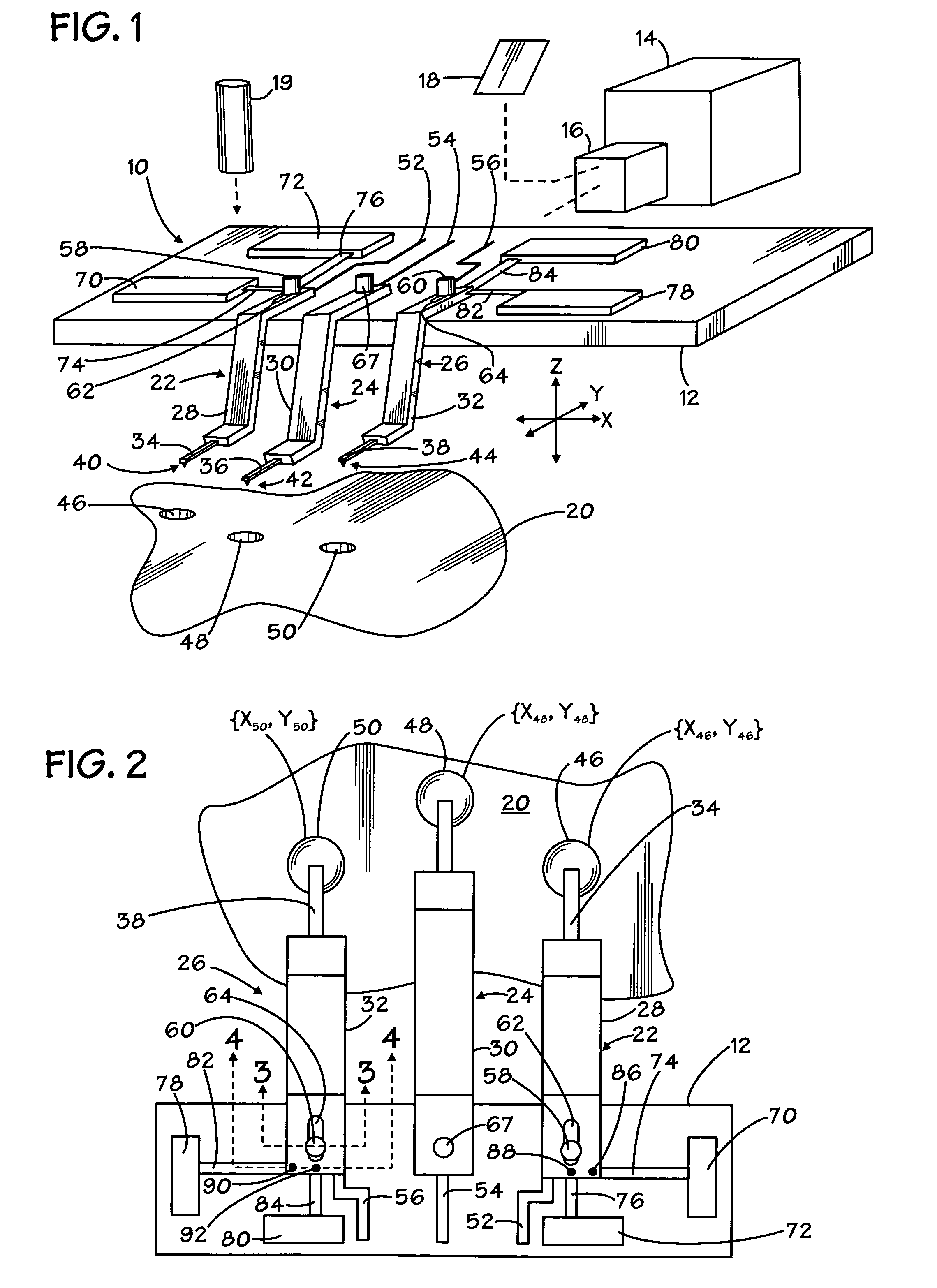
[0021]In the drawings described below, reference numerals are generally repeated where identical elements appear in more than one figure. Turning now to the drawings, FIGS. 1 and 2 depict a partially exploded pictorial view and a plan view of an exemplary embodiment of a probe system 10 that may utilize atomic force microscopy (“AFM”) in accordance with the present invention. The system 10 includes a base or cartridge 12 that is used in conjunction with an instrument 14. The instrument 14 is provided with an actuator 16 that engages the cartridge 12. A mirror 18 is coupled to the actuator 16. The instrument 14 is shown exploded from the cartridge 12 and the mirror 18 is shown exploded from the actuator 16. A laser source 19 is provided to illuminate selected portions of the cartridge 12. Light is reflected back up the mirror 18 and from there into the instrument. The function of the mirror 18 and laser source 19 will be described in more detail below.

[0022]The probe system 10 is des...


PUM


Abstract

Various probe systems and probes are provided. In one aspect, a probe is provided that includes a base and a first member coupled to the base. The first member has a first tip for probing a circuit device. A first actuator is coupled to the first member for moving the first member relative to the base. Electrical and/or topographical probing is possible.

Description

BACKGROUND OF THE INVENTION[0001]1. Field of the Invention[0002]This invention relates generally to semiconductor processing, and more particularly to electrical and / or atomic force microscopy probe systems.[0003]2. Description of the Related Art[0004]Atomic force microscopy (“AFM”) generally involves scanning a stylus or probe across a microscopic topography, such as an integrated circuit structure, and sensing the forces exerted on the stylus. The stylus is provided with a small geometry tip that physically contacts the surface topography. The tip may be made from conducting or semiconducting materials that enable various types of circuits to be electrically as well as topographically probed.[0005]The technique has been widely used in metrology of structures in photoresist, interlevel dielectric layers, sidewall angles, trench depths and surface morphology. The scanning resolution of the probe is dependent on the radius of curvature of the probe tip that contacts a given topograph...

Claims


Application Information

Patent Timeline
IPC IPC(8): B23Q17/09G01B5/28G01N19/02
CPCB82Y35/00G01Q70/06G01Q60/30
Inventor SANTANA, JR., MIGUELPOWELL, ROBERT
Owner GLOBALFOUNDRIES US INC
Why Eureka
Try Eureka