Stacked module systems and method

a technology of stacked modules and modules, applied in the field of stacked module systems and methods, can solve problems such as complex assembly problems

Active Publication Date: 2006-04-25
TAMIRAS PER PTE LTD LLC
View PDF423 Cites 89 Cited by
  • Summary
  • Abstract
  • Description
  • Claims
  • Application Information

AI Technical Summary

Problems solved by technology

A variety of previous techniques for stacking CSPs may present complex assembly problems.

Method used


Image

  • Stacked module systems and method
  • Stacked module systems and method
  • Stacked module systems and method

Examples


Embodiment Construction

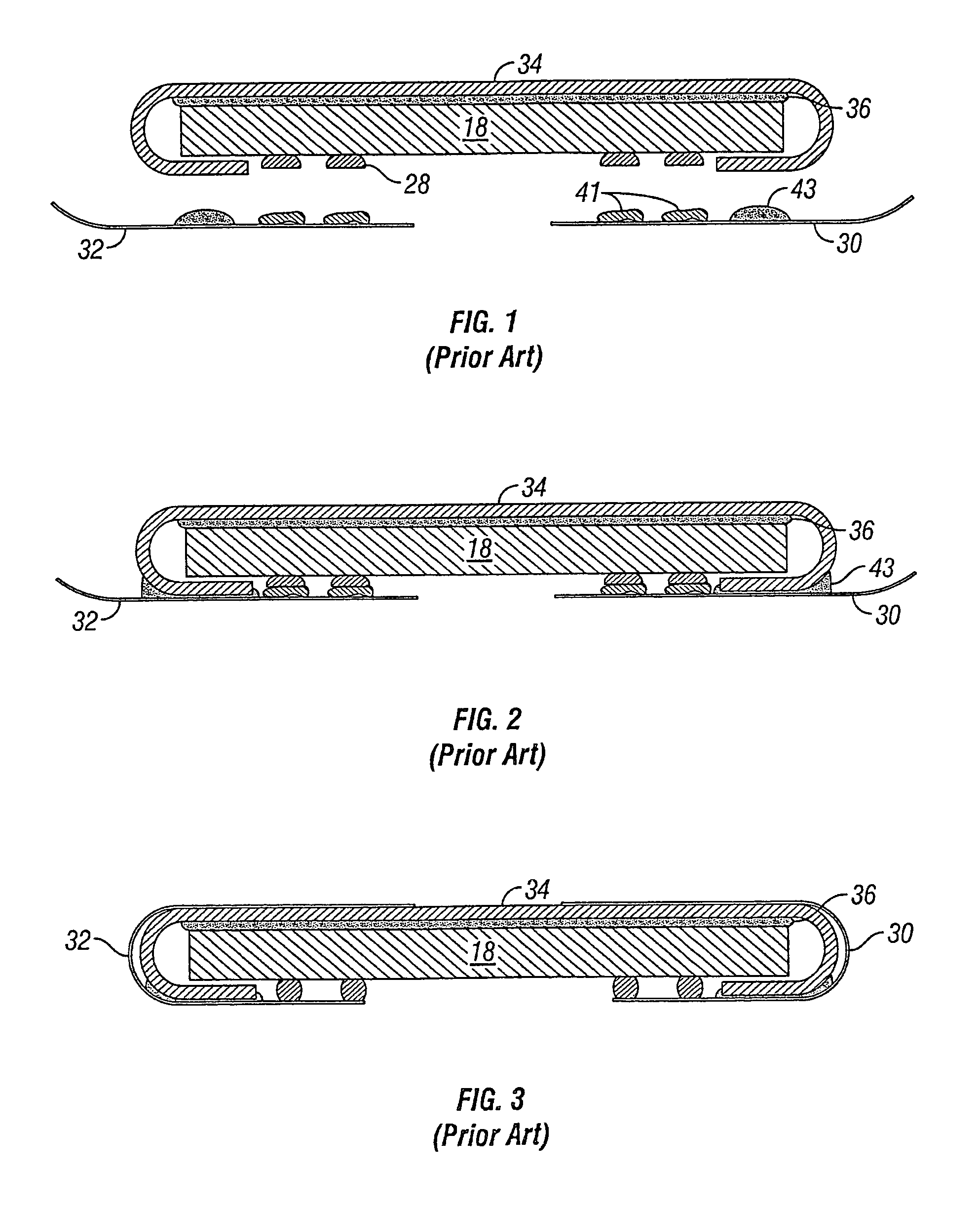
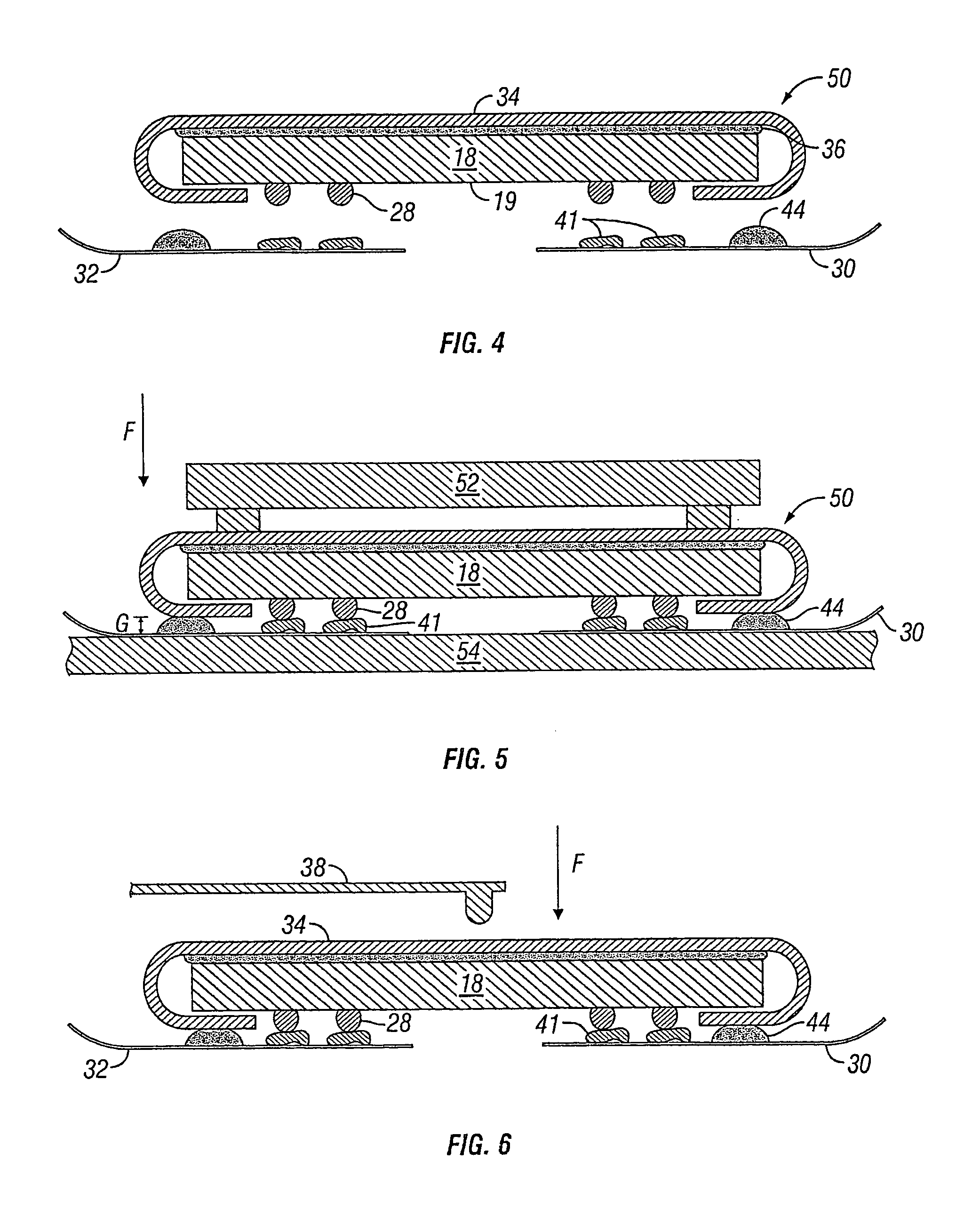
[0017]FIGS. 1–3 depict steps in a prior art method for constructing a high-density circuit module. FIG. 1 depicts a CSP 18 attached with adhesive 36 to form standard 34. In the configurations depicted, form standard 34 is devised to be employed with a CSP to provide a standard form for flex circuitry connector(s). Contacts 28 of CSP 18 have been compressed in a solid or semi-solid state and solder paste 41 and adhesive 43 have been applied to flex circuitry 30 and 32. FIG. 2 depicts a step in a prior art method for construction of a high-density module. Contacts 28 and solder paste sites 41 have come into contact as have form standard 34 and adhesive sites 43. FIG. 3 illustrates how solder paste sites 41 and compressed contacts 28 have merged to form solder joints and flex circuitry 30 and 32 has been wrapped about CSP 18.

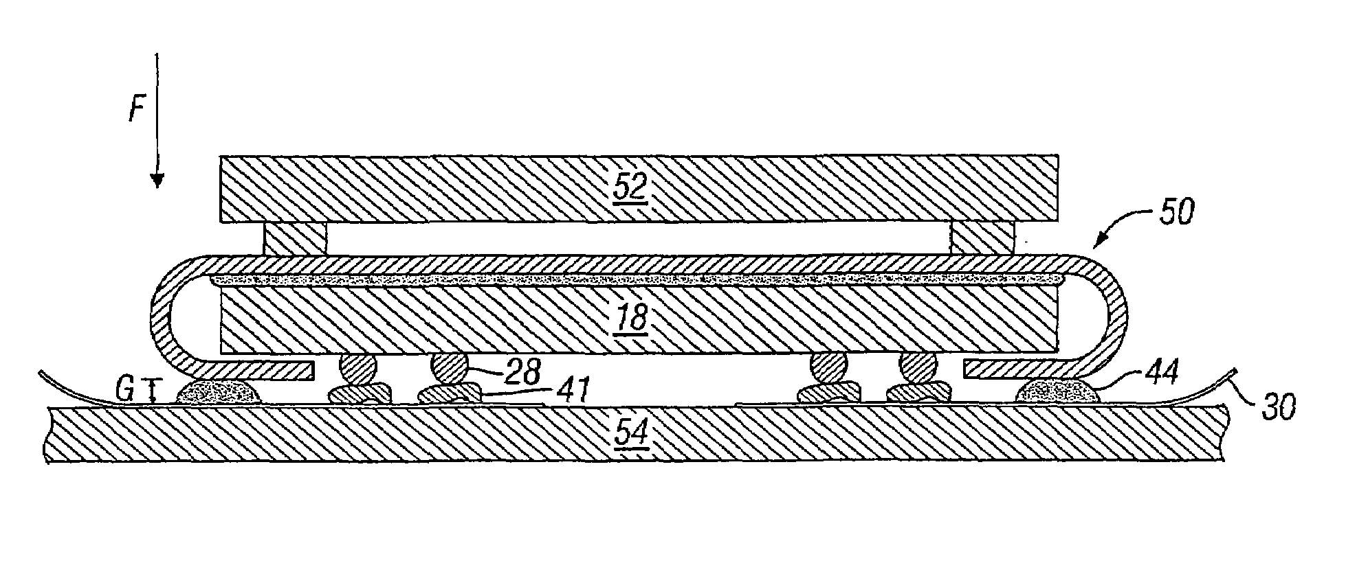
[0018]FIG. 4 depicts a method in accordance with a preferred embodiment of the present invention. CSP 18 and form standard 34 are attached with adhesive 36 to form...


PUM


Abstract

A combination composed from a form standard and a CSP is attached to flex circuitry. Solder paste is applied to first selected locations on the flex circuitry and adhesive is applied to second selected locations on the flex circuitry. The flex circuitry and the combination of the form standard and CSP are brought into proximity with each other. During solder reflow operation, a force is applied that tends to bring the combination and flex circuitry closer together. As the heat of solder reflow melts the contacts of the CSP, the combination collapses toward the flex circuitry displacing the adhesive as the solder paste and contacts merge into solder joints. In a preferred embodiment, the form standard will be devised of heat transference material, a metal, for example, such as copper would be preferred, to improve thermal performance. In other embodiments, the methods of the invention may be used to attach a CSP without a form standard to flex circuitry.

Description

RELATED APPLICATIONS[0001]U.S. patent application Ser. No. 10 / 453,398, filed Jun. 3, 2003, is hereby incorporated by reference.TECHNICAL FIELD[0002]The present invention relates to aggregating integrated circuits and, in particular, to methods for creating high density modules from chip-scale type devices.BACKGROUND OF THE INVENTION[0003]A variety of techniques are used to stack packaged integrated circuits. Some methods require special packages, while other techniques stack conventional packages.[0004]The predominant package configuration employed during the past decade has encapsulated an integrated circuit (IC) in a plastic surround typically having a rectangular configuration. The enveloped integrated circuit is connected to the application environment through leads emergent from the edge periphery of the plastic encapsulation. Such “leaded packages” have been the constituent elements most commonly employed by techniques for stacking packaged integrated circuits.[0005]Leaded pac...

Claims


Application Information

Patent Timeline
Patent Type & Authority Patents(United States)
IPC IPC(8): H01L21/44
CPCH01L25/105H01L25/50H05K3/3436H01L23/36H01L2224/73253H01L23/4985H05K1/189H05K3/305H05K2203/0278H01L2225/1041H01L2225/1058H01L2225/107H01L2224/16H01L2224/16225H01L2224/32225H01L23/49816H01L2924/00011H01L2924/00014Y02P70/50H01L2224/0401
Inventor PARTRIDGE, JULIANWEHRLY, JR., JAMES DOUGLASROPER, DAVID
Owner TAMIRAS PER PTE LTD LLC
Why Eureka
Try Eureka