Liquid crystal display and the manufacturing method thereof

a technology of liquid crystal display and manufacturing method, which is applied in the direction of instruments, non-linear optics, optics, etc., can solve the problems of liquid crystal degradation, down-grade display quality, and structure that requires excess materials, so as to avoid contamination and/or degradation of liquid crystal

Inactive Publication Date: 2006-05-02
NYTELL SOFTWARE LLC
View PDF3 Cites 19 Cited by
  • Summary
  • Abstract
  • Description
  • Claims
  • Application Information

AI Technical Summary

Benefits of technology

[0016]As embodied and broadly described herein, the invention provides a liquid crystal device (LCD), wherein the LCD includes a top and a bottom substrate in parallel, a sealant with which substrates thereof forming an enclosed space, and a liquid crystal layer forming within the enclosed space. When forming TFT and pixel electrode on inner surface of one of the substrates, a mask at least covers the deposited insulating layer and / or conductive layer in either step that forms the deposited insulating layer and / or conductive layer. Take another larger frame mask to simultaneously superimpose on one of the substrates to form a framing space in between the two masks, whereas the mask material is chosen depending on the insulating layer and the conductive layer, that is, a conductive material and insulating material respectively. Continue deposition in between the frame shape space so that deposition layer is formed. Remove the two masks after a predetermined period of time for deposition to form an enclosed liquid crystal wall so as to avoid contamination and / or degradation of liquid crystal.

Problems solved by technology

However, the drawback to this technique is, some part of the liquid crystal layer A4 would be exposed to lighting when irradiating sealant A3 in order to adhere substrates A1 to A2, thus liquid crystal suffers from degradation.
Moreover, the liquid crystal layer A4 that contacts with the sealant A3 is possibly contaminated, which also down-grades display quality.
Nevertheless, the structure requires excess materials and steps that complicate the process.
Obviously there is excess material cost and as well as the process has to be done after sealant is hardened.
Yet conductive material is required and the process difficulty is raised and all sealant B5 is possibly not hardened.

Method used


Image

  • Liquid crystal display and the manufacturing method thereof
  • Liquid crystal display and the manufacturing method thereof
  • Liquid crystal display and the manufacturing method thereof

Examples


first embodiment

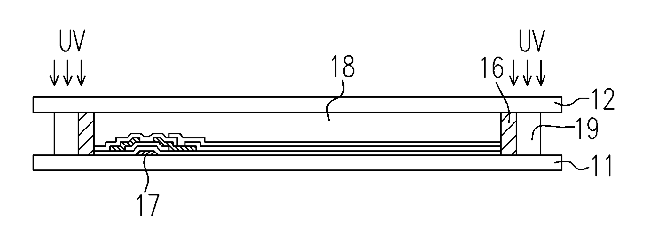
[0039 of the Present Invention: As shown in the FIGs. from 6A to 6F, a TFT formation process is performed on a substrate 11. To be simplified, only single TFT is illustrated in this and the other preferred embodiments in this invention. After depositing the gate metal layer 17, manipulate the mask 13 to at least cover the gate metal layer 17, and as well superimpose another larger frame mask 14 on the substrate 11 simultaneously. A frame spacing 15 (as shown in top view diagram in FIG. 6A) is formed in between the two masks, 13 and 14. The materials of masks 13 and 14 are those not prone to bond to metal, such as insulator, or processed material so that it does not prone to bond to metal. Notice that manipulation of masks 13 and 14 is automated.

[0040]As deposition is continued within the frame spacing 15 (as shown in FIG. 6B), an enclosed metal wall 16 is built after removal of the two masks 13 and 14 in a predetermined period of time. To accomplish the forming of the TFT (as shown ...


PUM

PropertyMeasurementUnit
conductiveaaaaaaaaaa
insulatingaaaaaaaaaa
structureaaaaaaaaaa

Abstract

A liquid crystal display device includes two parallel substrates spaced apart, a sealant forming an enclosed space with the two substrates and a liquid crystal layer forming in the enclosed space. After at least a conducting layer and / or an insulating layer of the Thin Film Transistors and the pixel electrodes thereon is deposited on the one substrate, two masks serve to at least cover the conducting layer and / or the insulating layer. As deposition is continued, at least one conducting and / or insulating wall structure with specific pattern on the one substrate is formed. Thus, contamination and degradation of the liquid crystal can be avoided and further the two substrates can be conducted without using conductive material.

Description

CROSS REFERENCE TO RELATED APPLICATIONS[0001]This application claims the priority benefit of Taiwan application serial no. 92116075, filed on Jun. 13, 2003.BACKGROUND OF INVENTION[0002]1. Field of Invention[0003]This invention relates to a liquid crystal device and the manufacturing method thereof. Moreover, this invention particularly relates to a liquid crystal device and manufacturing method for simultaneously forming conductive and / or insulating walls using Thin Film Transistor (TFT) Deposition as well as pixel electrode therein.[0004]2. Description of Prior Art[0005]The present liquid crystal device process comprises forming of Thin Film Transistor (TFT), Liquid Crystal Device (LCD) panel, and liquid crystal module. Common TFT structure includes gate metal layer, semiconductor layer (wherein semiconductor layer includes gate insulating layer, amorphous crystalline layer, and a n+ doping layer), source / drain metal layer, and passivation layer. The forming of TFT process includes...

Claims


Application Information

Patent Timeline
Patent Type & Authority Patents(United States)
IPC IPC(8): G02F1/1339G02F1/1345G02F1/1341G02F1/1368
CPCG02F1/1339G02F1/1341G02F2001/13415G02F1/13415
Inventor LEE, JIAHN-LIN
Owner NYTELL SOFTWARE LLC
Why Eureka
Try Eureka