Current sense amplifier circuits having a bias voltage node for adjusting input resistance

a current sense amplifier and input resistance technology, applied in the field of integrated circuit devices, can solve the problems of degrading limiting the operation environment of low voltage and reducing the operation stability of conventional current sense amplifiers

Inactive Publication Date: 2006-05-02
SAMSUNG ELECTRONICS CO LTD
View PDF10 Cites 45 Cited by
  • Summary
  • Abstract
  • Description
  • Claims
  • Application Information

AI Technical Summary

Problems solved by technology

Unfortunately, conventional current sense amplifiers may be restricted to low voltage operation environments.
Moreover, conventional current sense amplifiers may experience degradation in operation stability and / or sensing delay increases.
If RIN1 and M2 constituting the cross-coupled latch circuit is larger than that of the current source transistors M3 and M4 preventing the latch operation, then the column selection line CSL may have similar properties as a latch, which may degrade operation stability.
Unfortunately, data transmission speed may be reduced because a voltage difference is generated between two inputs of the column selection line CSL.
However, although RIN=0 may be met under particular conditions, variation of the operation voltage or the operation temperature may prevent the result of RIN=0 from being met.
Operation at low voltage, however, may prevent each of the transistors of the column selection line CSL from maintaining its saturation mode, which may result in a greater change in RIN.
Accordingly, ideal column selection line CSL functionality may be lost.
Two problems may arise in this case.
Further, because the voltages on the output nodes SO and / SO become inputs to the differential amplifier 30 connected to a next stage, it may degrade the operation speed of the differential amplifier.
Because the voltages on the sensing outputs SO and / SO change, sensing delay may increase.
If the transistors constituting the current sense amplifier 20 are changed in size for the input resistance RIN of the column selection line CSL at the low voltage to be zero, then the input resistance RIN becomes negative (−) when VDD is high, which may cause a stability problem.
In addition, the output voltage swing of the current sense amplifier 20 (voltage swing at the SO and / SO nodes) may be reduced depending on the increase of the input resistance RIN of the column selection line CSL, which may cause a problem in that the sensing delay further increases.
However, there is still a problem that the change in the input resistance RIN becomes greater because the PMOS transistors constituting the cross-coupled latch and the NMOS transistors for latch prevention have a current pass characteristic difference therebetween due to PVT variation.

Method used


Image

  • Current sense amplifier circuits having a bias voltage node for adjusting input resistance
  • Current sense amplifier circuits having a bias voltage node for adjusting input resistance
  • Current sense amplifier circuits having a bias voltage node for adjusting input resistance

Examples


Embodiment Construction

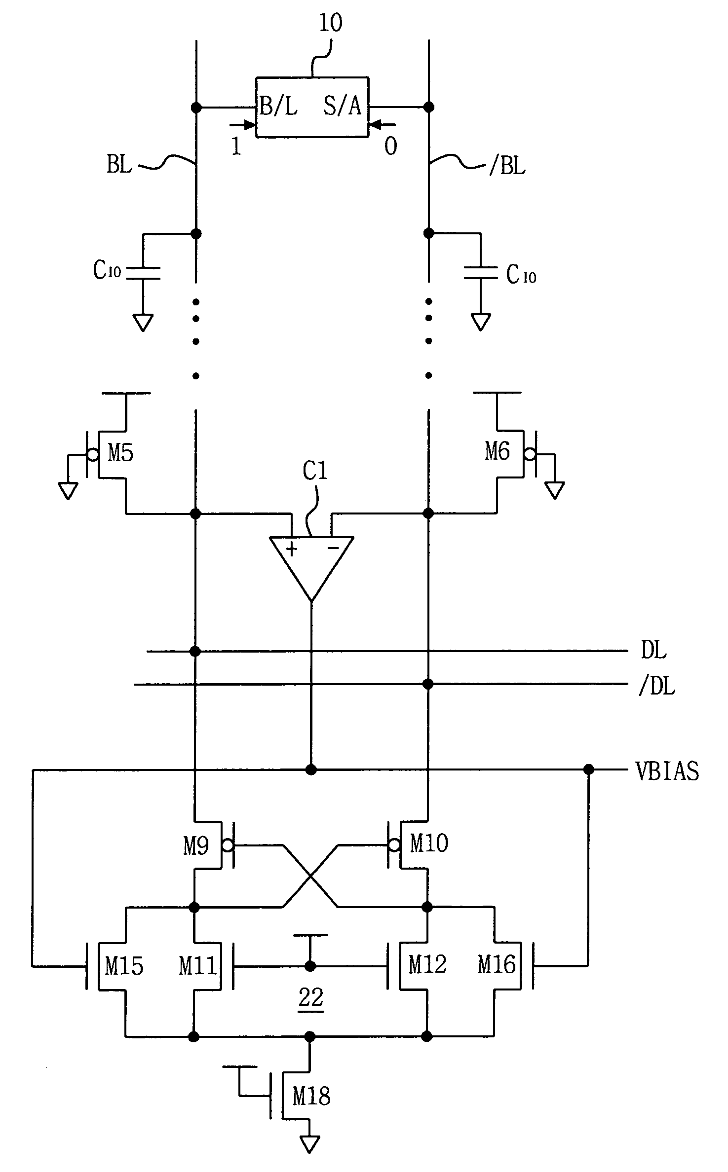
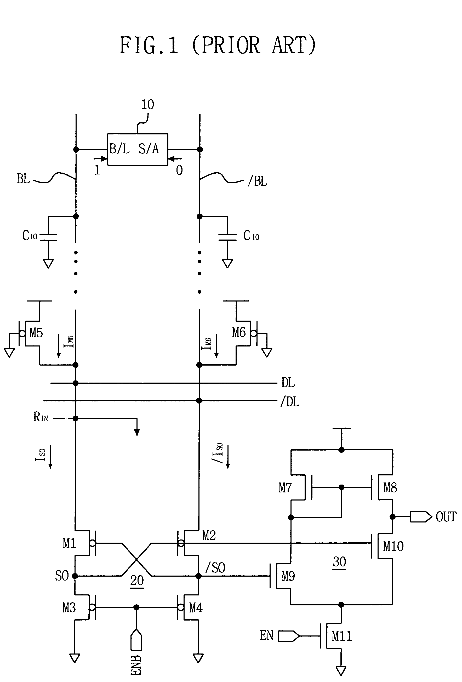
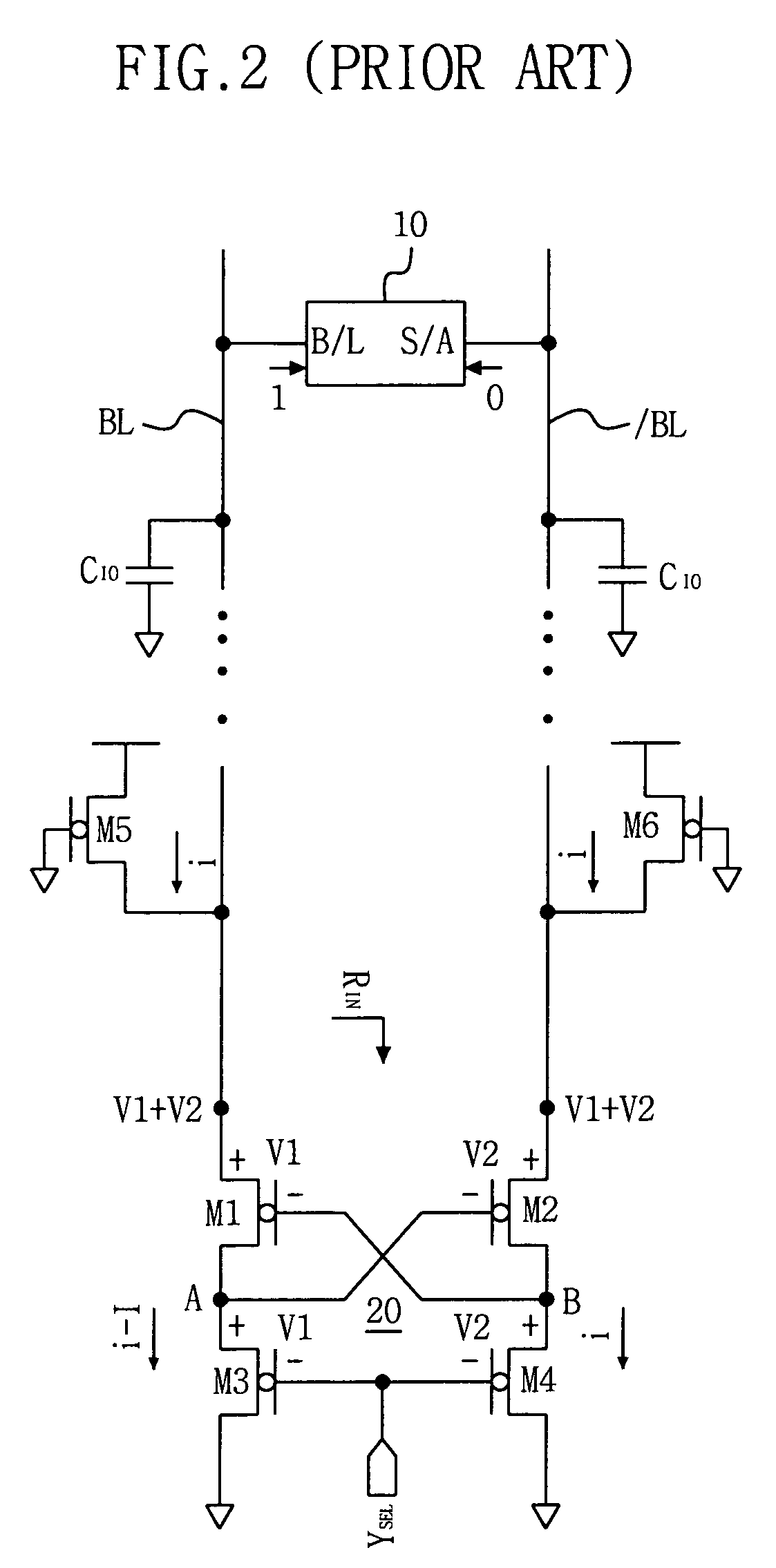
[0038]While the invention is susceptible to various modifications and alternative forms, specific embodiments thereof are shown by way of example in the drawings and will herein be described in detail. It should be understood, however, that there is no intent to limit the invention to the particular forms disclosed, but on the contrary, the invention is to cover all modifications, equivalents, and alternatives falling within the spirit and scope of the invention as defined by the claims. Like reference numbers signify like elements throughout the description of the figures.

[0039]As used herein, the singular forms “a,”“an,” and “the” are intended to include the plural forms as well, unless expressly stated otherwise. It will be further understood that the terms “includes,”“comprises,”“including,” and / or “comprising,” when used in this specification, specify the presence of stated features, integers, steps, operations, elements, and / or components, but do not preclude the presence or a...


PUM


Abstract

A current sense amplifier includes first and second P type MOS transistors having source nodes connected to first and second sensing inputs, respectively, and gate and drain nodes being cross-coupled to each other. First and second N type MOS transistors have drain nodes connected to first and second sensing outputs, respectively, the first and second sensing outputs corresponding to the drain nodes of the first and second P type MOS transistors, respectively, the first and second N type MOS transistors having respective gate nodes connected to a power supply voltage. Third and fourth N type MOS transistors have drain nodes connected to the first and second sensing outputs, respectively, and gate nodes connected to a bias voltage node so that respective current paths are established from the first and second sensing outputs to a common reference node.

Description

RELATED APPLICATION[0001]This application claims the benefit of and priority to Korean Patent Application No. 2004-14234, filed Mar. 3, 2004, the disclosure of which is hereby incorporated herein by reference.FIELD OF THE INVENTION[0002]The present invention relates generally to integrated circuit devices and methods of operating the same and, more particularly, to integrated circuit memory devices that incorporate a sense amplifier circuit and methods of operating the same.BACKGROUND OF THE INVENTION[0003]Generally, as a chip size of a semiconductor memory increases, a length of a data line that is used for transporting data increases as well. Accordingly, a current sense amplifier, which may be relatively less influenced from capacitive loads of data lines as compared to a voltage sense amplifier, may be used in semiconductor memory devices. In a current sense amplifier, because it does not have voltage a difference on data lines, the data lines need not be equalized even when dif...

Claims


Application Information

Patent Timeline
Patent Type & Authority Patents(United States)
IPC IPC(8): G11C7/02G11C11/4091G11C7/06G11C11/419
CPCG11C11/4091G11C7/04G11C7/06
Inventor LEE, SANG-BO
Owner SAMSUNG ELECTRONICS CO LTD
Why Eureka
Try Eureka