

Memory mapped I/O bus selection
a memory-mapped and bus-type technology, applied in the field of i/o bus-type structures, can solve the problem of more expensive asic manufacturing
- Summary
- Abstract
- Description
- Claims
- Application Information
AI Technical Summary
Problems solved by technology
Method used
Image

Examples
Embodiment Construction
[0025]While the present invention is described herein with reference to illustrative embodiments for particular applications, it should be understood that the invention is not limited thereto. Those skilled in the art(s) with access to the teachings provided herein will recognize additional modifications, applications, and embodiments within the scope thereof and additional fields in which the present invention would be of significant utility.
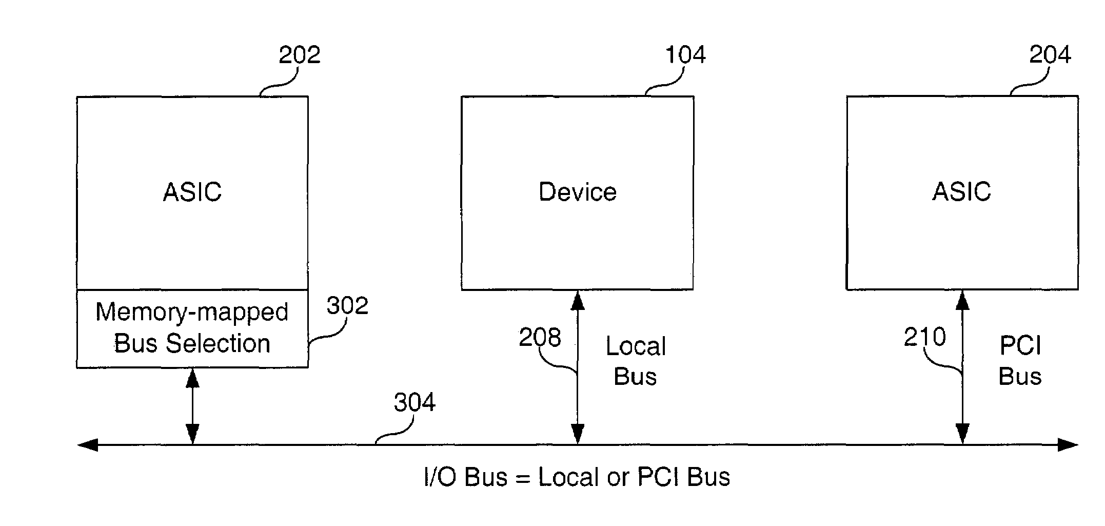
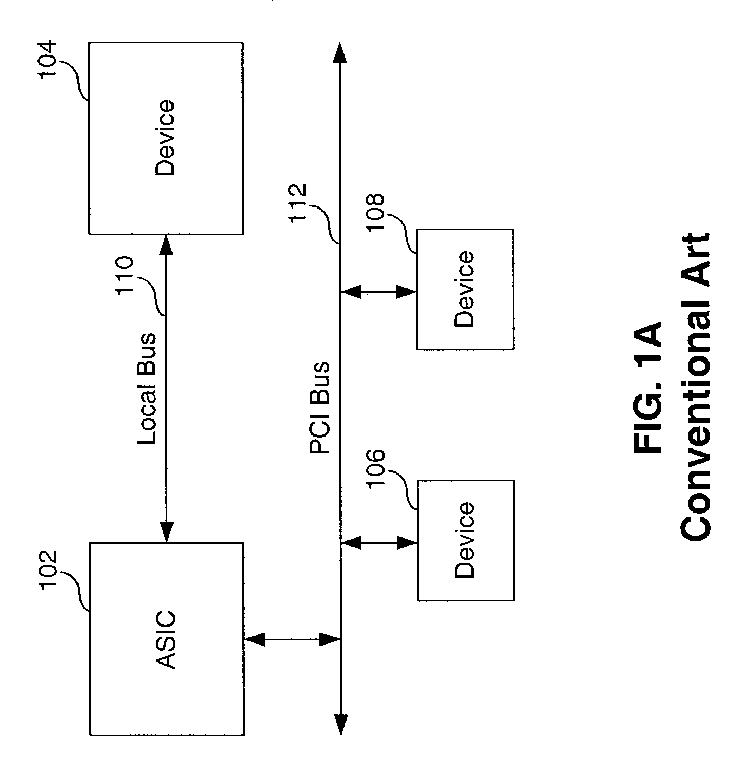
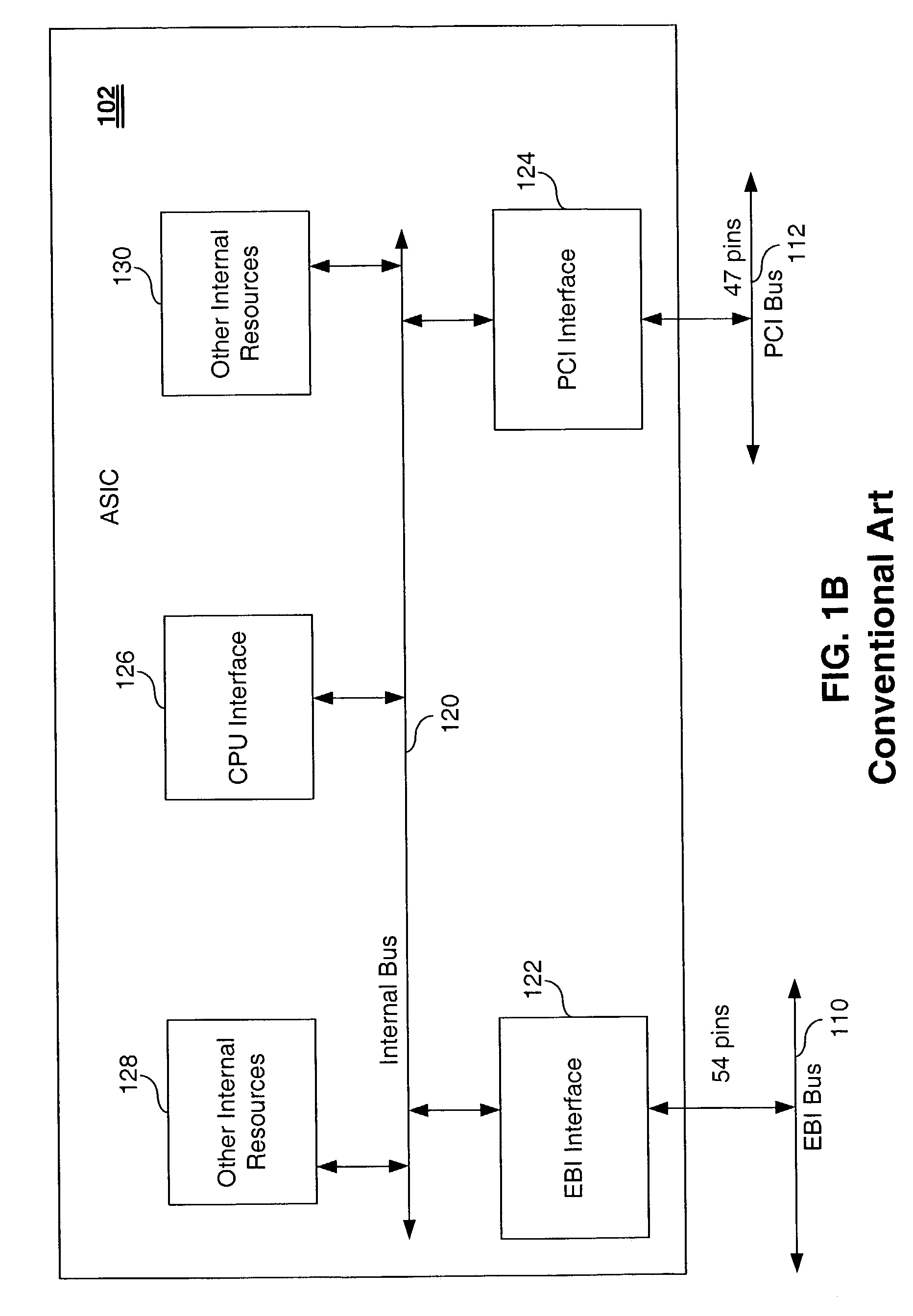
[0026]The present invention is directed to a mechanism and method for redefining an application specific integrated circuit's I / O bus structure in real-time. The mechanism includes an address map block, a state machine block, and a bus arbitration block. At initialization, the address map is configured to divide the address space into regions (i.e., used for bus addressing, used for other purposes, see generally FIG. 6) and type of bus structure (e.g., PCI, EBI, etc.). When I / O access is requested by a client (e.g., CPU, DMA controller, etc.), ...
PUM
 Abstract
Description
Claims
Application Information