Non-contact IC card having enhanced reliability

a non-contact, ic card technology, applied in the direction of instruments, printing, semiconductor/solid-state device details, etc., can solve the problems of excessive failure rate of non-contact ic cards, damage to ic chips, and inability to operate, etc., to achieve the effect of enhancing reliability

Inactive Publication Date: 2006-05-16
DENSO WAVE INC
View PDF6 Cites 30 Cited by
  • Summary
  • Abstract
  • Description
  • Claims
  • Application Information

AI Technical Summary

Benefits of technology

[0006]It is an objective of the present invention to overcome the above problem by providing a non-contact IC card having enhanced reliability, due to being less susceptible to damage resulting from application of an external force.
[0007]To achieve the above objective, firstly, a non-contact IC card according to the present invention is provided with two independent combinations of an IC chip and an antenna coil which is connected to that IC chip. Since there are two chips, each of which has stored therein the same set of necessary data (e.g. a key code, for use in unlocking a door) the probability of the IC card becoming inoperable due to application of external force becomes substantially reduced. That is to say, it is unlikely that both of the IC chips will be destroyed simultaneously. Hence, the reliability of such a non-contact IC card for use in an application such as a door key is substantially increased.
[0008]Secondly, such a non-contact IC card can be manufactured by mounting one combination of an IC chip and the corresponding antenna coil one of a pair of sheets of a material that is suitable as the outer cover of an IC card, and mounting the other combination of IC chip and antenna coil on the second one of these sheets. By attaching these sheets with the IC chips and antenna coils enclosed between them, such a non-contact IC card can be easily manufactured.

Problems solved by technology

With such a prior art type of non-contact IC card, since the IC chip is in the form of a bare chip, the IC chip may become damaged and thereby inoperative, if an external force is applied to the card.
However even when such a measure is adopted, the failure rate of such non-contact IC cards is excessively high, being approximately 1%.
Such a high failure rate signifies that a sufficiently high degree of reliability cannot be obtained for such non-contact IC cards when these are used in such applications as keys for unlocking vehicle doors or house doors.

Method used


Image

  • Non-contact IC card having enhanced reliability
  • Non-contact IC card having enhanced reliability
  • Non-contact IC card having enhanced reliability

Examples


second embodiment

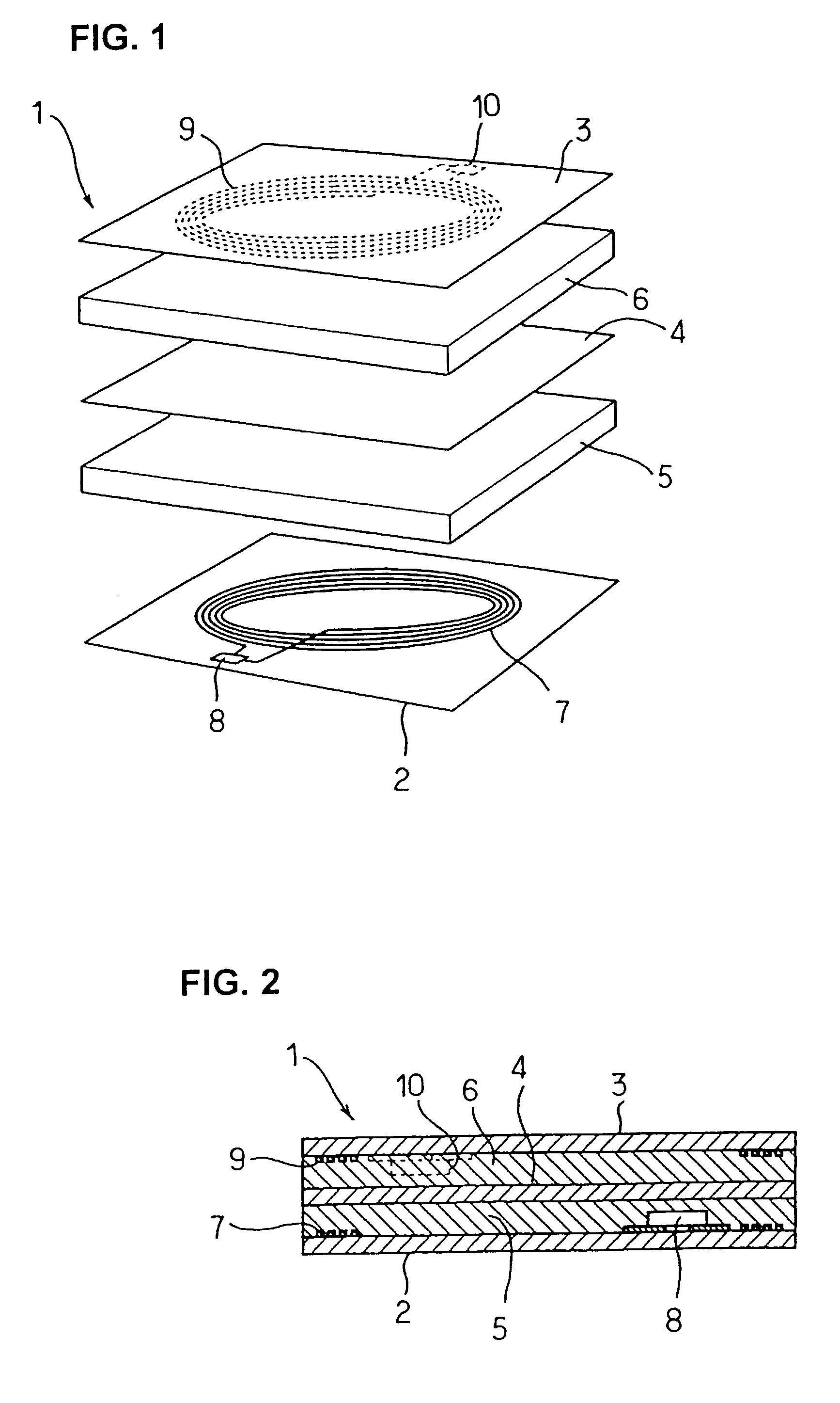
[0047]FIGS. 4A to 4F are diagrams for illustrating a manufacturing process for a second embodiment of a non-contact IC card. Components of this embodiment which are identical to those of the first embodiment are indicated by correspondingly identical reference numerals.

[0048]With the second embodiment both of the combinations of the antenna coil 7, IC chip 8 and the antenna coil 9, IC chip 10, are mounted in common on the same one of the two plastic sheets 2, 3 which constitute the covering of the non-contact IC card. In this case it is assumed that both combinations are mounted on sheet 2.

[0049]The manufacturing process is as follows. Firstly, as shown in FIG. 4A, one of the antenna coils (antenna coil 7) is formed on the upper face of the sheet 2 by a screen printing process using an electrically conductive paste. Next, as shown in FIG. 4B, an electrically insulating layer 11 is formed over the antenna coil 7 on the upper face of the sheet 2, by a printing process using an electri...

third embodiment

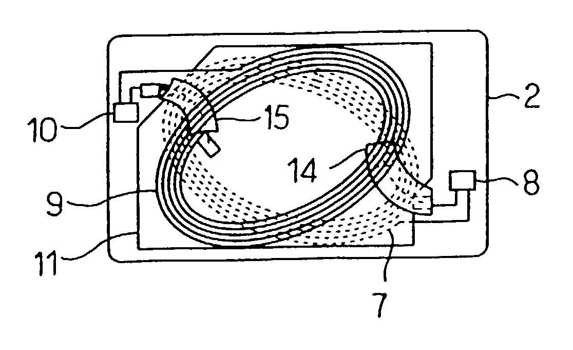
[0053]FIG. 5 is a plan view illustrating a third embodiment of a non-contact IC card (as seen with the sheet 3 removed). Components of this embodiment which are identical to those of the second embodiment are indicated by correspondingly identical reference numerals. With this embodiment, as shown in FIG. 5, both the antenna coils 7 and 9 and the IC chips 8, 10 are formed on the same one of the two sheets 2, 3 which form the cover of the card (in this example, on sheet 2). However the antenna coil 9 and IC chip 10 are disposed within the inner periphery of the antenna coil 7, with the IC chip 8 disposed at the outer periphery of the antenna coil 7.

[0054]With the third embodiment, since the configuration of the non-contact IC card is similar to that of the second embodiment, similar advantages are obtained to those described hereinabove for the second embodiment.

fourth embodiment

[0055]FIG. 6 is a plan view illustrating a fourth embodiment of a non-contact IC card (as seen with the sheet 3 removed). Components of this embodiment which are identical to those of the third embodiment are indicated by correspondingly identical reference numerals. With this embodiment, as shown in FIG. 6, the antenna coil 7 and IC chip 8 are mounted in a region which occupies approximately half of the upper face of one of the two sheets 2, 3 (in this example, sheet 2) while the antenna coil 7 and IC chip 8 are mounted in a region which occupies the remaining half of that upper face of sheet 2.

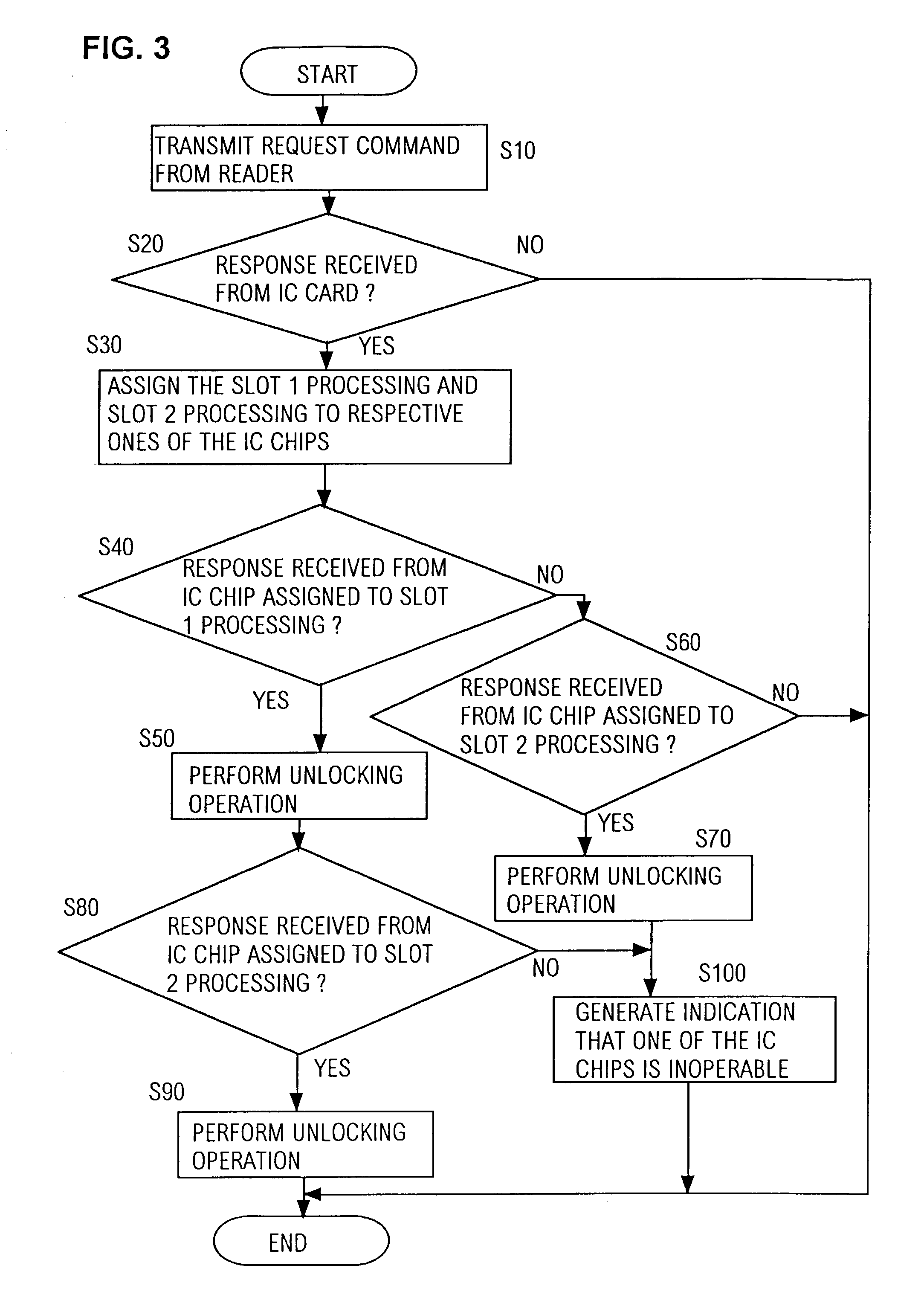
[0056]With the fourth embodiment, it becomes possible to configure the IC card read / write apparatus with an antenna coil arrangement which matches that of the antenna coils 7, 9 of a non-contact IC card 1. In that case, it would be possible for the IC card read / write apparatus to concurrently perform mutually independent transmitting / receiving of data for both the IC chips 8, 10 of a card 1....


PUM


Abstract

To increase the reliability of a non-contact IC card for use in such applications as a door key, etc., two separate combinations of an IC chip and an antenna coil coupled to that chip are provided in the card, with each IC chip storing the same information, such as a key code. Since the probability of both of the IC chips being damaged concurrently due to application of external force is much smaller than the probability of failure of a single IC chip, the objective of enhanced reliability is effectively achieved.

Description

BACKGROUND OF THE INVENTION[0001]1. Field of Technology[0002]The present invention relates to a non-contact IC (integrated circuit) card having an IC chip and an antenna coil which is connected to the IC chip.[0003]2. Related Prior Art[0004]A non-contact IC card is generally formed with an external cover consisting of two sheets of thin film of an electrically insulating material, an intermediate layer of an attachment material for mutually attaching these sheets, and an antenna coil and an IC chip which are mounted on an inner face of one of the sheets.[0005]With such a prior art type of non-contact IC card, since the IC chip is in the form of a bare chip, the IC chip may become damaged and thereby inoperative, if an external force is applied to the card. For that reason, a reinforcing plate is usually incorporated, mounted over the IC chip, to strengthen the IC chip. However even when such a measure is adopted, the failure rate of such non-contact IC cards is excessively high, bei...

Claims


Application Information

Patent Timeline
Patent Type & Authority Patents(United States)
IPC IPC(8): G06K19/06B42D15/10G06K19/07G06K19/077H01L23/498H01L23/64
CPCG06K19/072G06K19/07728G06K19/07749G06K19/07767H01L23/49855H01L23/645H01L2924/0002H01L2223/6677H01L2924/00
Inventor KAMIYA, MSASHIWATANABE, ATSUSHI
Owner DENSO WAVE INC
Why Eureka
Try Eureka