Electronic component having micro-electrical mechanical system

a mechanical system and micro-electric technology, applied in the direction of acceleration measurement using interia force, instrumentation, device material selection, etc., can solve the problems of difficult to keep the mechanical strength of the si substrate, difficult to form the opening in a predetermined size in a predetermined position on the upper surface of the substrate accurately, and little design freedom

Active Publication Date: 2006-05-30
KIOXIA CORP
View PDF6 Cites 151 Cited by
  • Summary
  • Abstract
  • Description
  • Claims
  • Application Information

AI Technical Summary

Problems solved by technology

In this process, since the size of the space for movement of the MEMS element is restricted by the thickness of the sacrifice layer, there is little freedom for the design.
Consequently, with regard to the “Bulk MEMS process” where the Si substrate is etched from the lower surface thereof, it is difficult to form the opening in a predetermined size in a predetermined position in the upper surface of the substrate accurately.
In addition, since a cavity larger than necessary is formed in the Si substrate, it is difficult to keep the mechanical strength of the Si substrate.
However, when using a component called an RF-MEMS, which is used in the communication field (a switch, a filter, a variable inductor, a variable capacity, an antenna, etc.), there are cases where a parasitic capacitance and inductance are caused by the wire bonding and thus the intended performance cannot be attained.
Thus, unlike conventional general-purpose packages, resin molding cannot be performed.
Because of the inconsistency between the mounting processes, it is difficult to manufacture an SIP (System In Package), wherein an MEMS element and other circuit chips are integrated in one package, and thus the MEMS element is usually mounted on a board as an isolated device.

Method used


Image

  • Electronic component having micro-electrical mechanical system
  • Electronic component having micro-electrical mechanical system
  • Electronic component having micro-electrical mechanical system

Examples


first embodiment

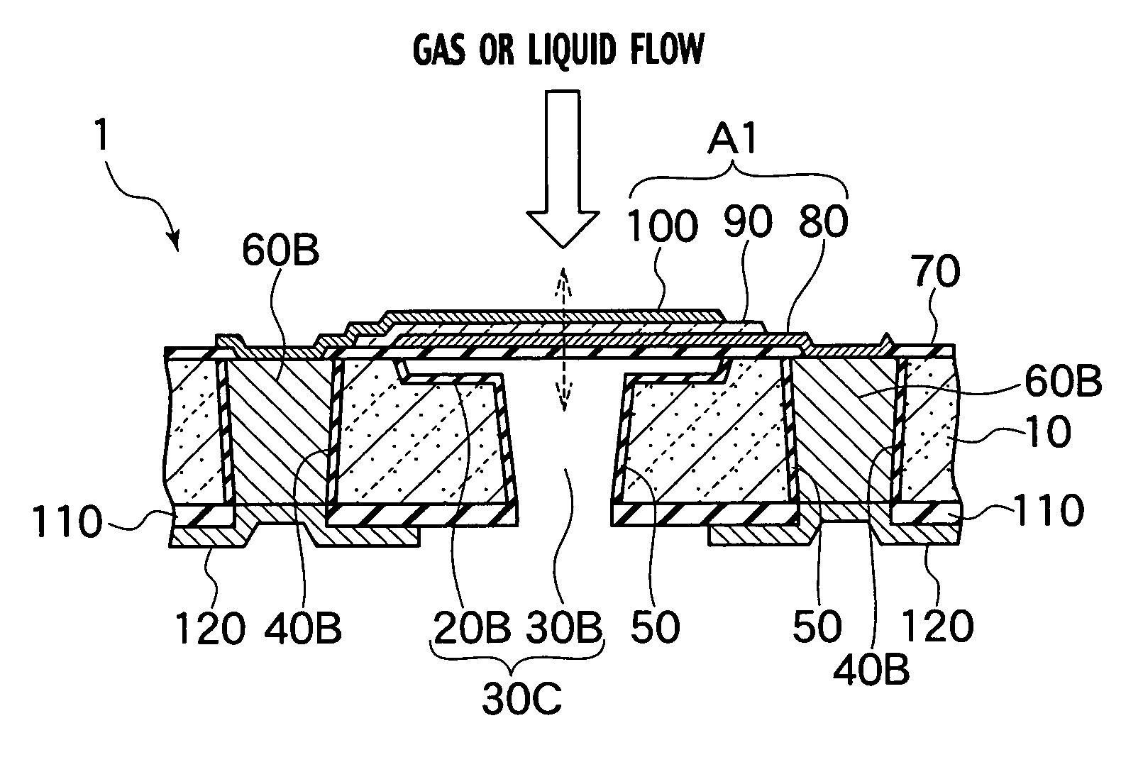
[0027]In FIG. 1A, a structure of an MEMS electronic component 1 according to the first embodiment is shown. As shown in FIG. 1A, the MEMS electronic component 1 according to the first embodiment includes an MEMS element (an electrical mechanical element) A1, which has a movable portion in an upper surface (or a first electrode) of a silicon substrate 10. The first embodiment illustrates a piezoelectric device, as the MEMS element A1, which can be used as a thin film bulk acoustics resonator (FBAR), various sensors, etc. The piezoelectric device has a structure where a piezo-electric film 90 is sandwiched between the upper electrode 100 and a lower electrode (or a second electrode) 80. The piezo-electric film 90 moves in the vertical direction shown by a broken-line arrow, and in the in-planar direction of the substrate plane.

[0028]The MEMS electronic component 1 according to the first embodiment has a cavity 30C, which penetrates from an upper surface (or a first surface) to a lower...

second embodiment

[0055]A structure of a MEMS electronic component 3 according to the second embodiment is shown in FIG. 5.

[0056]As shown in this drawing, like the MEMS electronic component 1 according to the first embodiment, the MEMS electronic component 3 according to the second embodiment includes a MEMS element A2 with a movable portion on the upper surface of a silicon substrate 11. The MEMS electronic component 3 also includes a cavity 31B, which penetrates between the upper surface and the lower surface of the silicon substrate 11, in the region corresponding to the mechanical movable portion of the MEMS element A2. Further, the MEMS electronic component 3 includes an electric conduction plug 61B penetrating between the upper surface and the lower surface of the silicon substrate 11, which is assigned as a lead electrode of the MEMS element A2. The variations in structure from the MEMS electronic component 1 according to the first embodiment are as follows. First, unlike the first embodiment,...

third embodiment

[0069]The third embodiment is a modification of the second embodiment. Although the structure of the MEMS electronic component has almost the same structure as the one shown in FIG. 5, the space for movement for the MEMS element and the subsequent trench formation step of forming the cavity portion are different.

[0070]Steps of manufacturing the trench 31A, which is the characterizing portion according to the third embodiment, is shown in FIG. 7A and FIG. 7B. In addition, FIG. 7A and FIG. 7B show cross sectional views at 7B—7B line of a plan view shown in FIG. 7C.

[0071]As shown in FIG. 7A, a shallow trench 21 is formed for securing the space for movement of the MEMS element in the silicon substrate 11. Next, resist 200 is patterned to form an etching mask, and an etching residual pattern 210 in the shape of a convex is formed in the trench 31A using this etching mask, as shown in FIG. 7B. With the presence of this etching residual pattern 210 in the shape of a convex, the amount of t...


PUM

PropertyMeasurementUnit
angleaaaaaaaaaa
depthaaaaaaaaaa
depthaaaaaaaaaa

Abstract

An electronic component includes a semiconductor substrate having a first surface and a second surface opposite to the first surface, a cavity that penetrates from the first surface to the second surface of the semiconductor substrate, and an electrical mechanical element that has a movable portion formed above the first surface of the semiconductor substrate so that the movable portion is arranged above the cavity. The electronic component further includes an electric conduction plug, which penetrates from the first surface to the second surface of the semiconductor substrate, and which is electrically connected to the electrical mechanical element.

Description

CROSS REFERENCE TO RELATED APPLICATIONS[0001]This application is based upon and claims the benefit of priority from the prior Japanese Patent Application No. 2004-106204 filed on Mar. 31, 2004, the entire contents of which are incorporated herein by reference.BACKGROUND OF THE INVENTION[0002]1. Field of the Present Invention[0003]This invention relates to an electronic component, and an electronic component module, including a MEMS (Micro-Electrical Mechanical System) which is a micro device having an electric function and a mechanical function, and to a method of manufacturing the electronic component.[0004]2. Description of the Related Art[0005]An electronic component having a micro electrical mechanical element has been developed. (Hereinafter, the electronic components and the micro electrical mechanical element are referred to as “MEMS electronic components” and a “MEMS element” respectively.) There have been recent active studies of the MEMS electronic components that use a ma...

Claims


Application Information

Patent Timeline
Patent Type & Authority Patents(United States)
IPC IPC(8): H01L29/82H01L41/09B81B3/00B81B7/00G01L9/00G01P15/08G01P15/09H01L21/00H01L37/02H01L41/08H01L41/113H01L41/18H01L41/187H01L41/193H01L41/22H03H3/02H03H9/10H03H9/17
CPCB81C1/00095B81C1/0023G01L9/0019G01P15/0802G01P15/0922G01P15/18H01L41/1132H03H3/02H03H9/105H03H9/174H01L41/316H01L41/332H01L37/02H01L21/76898G01P2015/084H01L2224/16225H10N15/10H10N30/302H10N30/076H10N30/082
Inventor MATSUO, MIE
Owner KIOXIA CORP
Why Eureka
Try Eureka