Avalanche diode with breakdown voltage controlled by gate length

a technology of diodes and breakdown voltage, applied in the direction of basic electric elements, electrical apparatus, semiconductor devices, etc., can solve the problem that the polygate structure of the present diode cannot be provided

Inactive Publication Date: 2006-06-06
NAT SEMICON CORP
View PDF1 Cites 24 Cited by
  • Summary
  • Abstract
  • Description
  • Claims
  • Application Information

AI Technical Summary

Problems solved by technology

However, the polygate of the present diode structure need not necessarily be provided with a contact.

Method used


Image

  • Avalanche diode with breakdown voltage controlled by gate length
  • Avalanche diode with breakdown voltage controlled by gate length
  • Avalanche diode with breakdown voltage controlled by gate length

Examples


Embodiment Construction

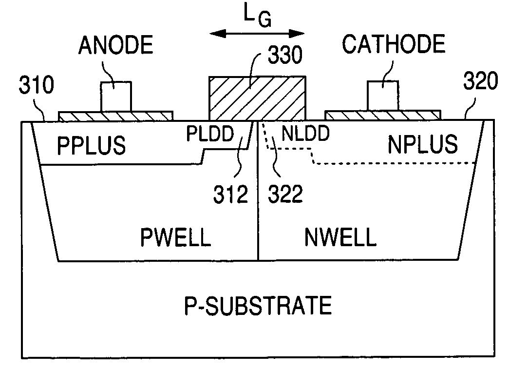
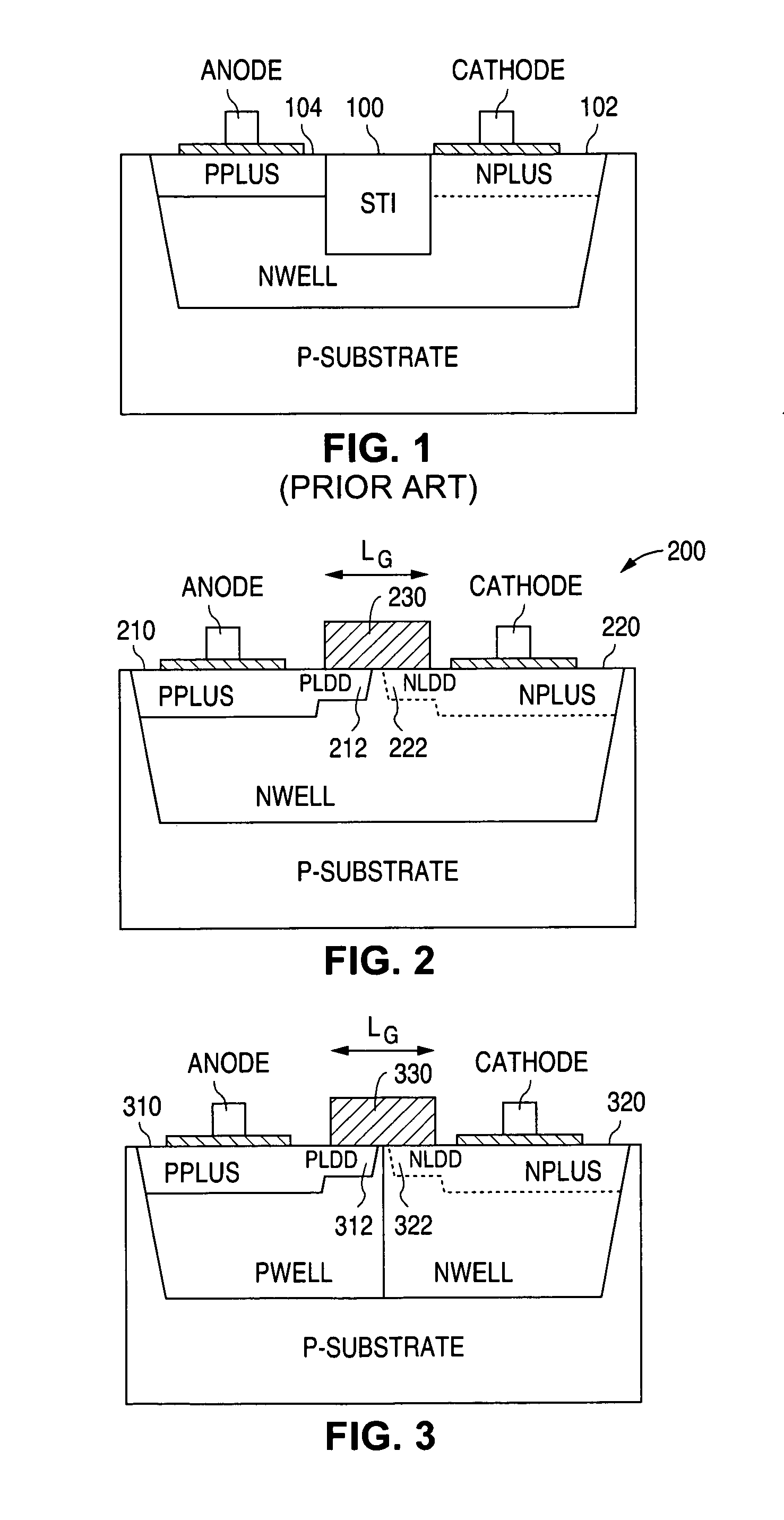
[0016]One embodiment of the invention is shown in FIG. 2 which shows the p-n junction of the diode 200 formed between a p+ region 210 formed in a lightly doped region 212 referred to as a p-lightly doped drain (PLDD), and a n+ region 220 formed in a lightly doped region 222 referred to as a n-lightly doped drain (NLDD).

[0017]The need for the PLDD and NLDD regions 212, 222 can be ascribed to the CMOS process. In order to avoid contamination across the junction during the high doping process, the formation of the p+ and n+ regions 210, 220 is typically preceded by the formation of lightly doped regions, referred to as PLDD (p-lightly doped region) and NLDD (n-lightly doped region), respectively.

[0018]As is evident from FIG. 2, a polygate 230 is formed over the region where the p-n junction will be located. The polygate 230 has a self aligning mask function. Even though separate masks are used during the doping of the p+ and PLDD and n+ and NLDD regions, it becomes difficult to properl...


PUM


Abstract

In an avalanche structure, different breakdown voltages are achieved by making use of a polygate and forming a highly doped p-n junction beneath the polygate, and adjusting the gate length and optionally the bias voltage of the gate.

Description

BACKGROUND OF THE INVENTION[0001]Avalanche diodes, which are sometimes loosely referred to as Zener diodes are commonly used for providing a reference voltages for analog circuits. One particular application is as part of an ESD protection clamp.[0002]An important consideration in designing semiconductor circuits, however, is the need to avoid introducing special process steps that would increase the overall cost. Thus it is desirable to be able to include so-called free structures by making use of existing process steps. In a CMOS process, however, only limited variations can be made to available regions in order to form diodes. For instance, diodes can be created using n+ / p-well, p+ / n-well, p-well / n-well, and, to some extent, n+ / p+ junctions by spacing the n+ and p+ regions far apart to avoid tunneling. In a 0.18 um process these combinations typically provide breakdown voltages of approximately 12V, 12V, 17V, and 4V, respectively. As a result avalanche diodes are available only w...

Claims


Application Information

Patent Timeline
Patent Type & Authority Patents(United States)
IPC IPC(8): H01L21/00H01L21/20
CPCH01L29/7391H01L29/866Y10S438/979Y10S438/983
Inventor VASHCHENKO, VLADISLAVCONCANNON, ANNHOPPET, PETER J.TER BEEK, MARCEL
Owner NAT SEMICON CORP
Why Eureka
Try Eureka