Components, methods and assemblies for multi-chip packages

a multi-chip module and assembly technology, applied in the direction of printed circuit manufacturing, printed circuit aspects, semiconductor/solid-state device details, etc., can solve the problems of increasing the consuming additional space for circuit panels and main circuit boards, and difficult to repair, let alone test, and improving the test and repair capabilities of multi-chip modules. , the effect of low overall height of the mcm

Active Publication Date: 2006-06-13
TESSERA INC
View PDF46 Cites 43 Cited by
  • Summary
  • Abstract
  • Description
  • Claims
  • Application Information

AI Technical Summary

Benefits of technology

The invention is a way to connect semiconductor chips to an interposer using a special connection method called land grid array (LGA). This method allows for a thinner overall height of the connection, and also improves the testing and repair of the chips.

Problems solved by technology

The technical problem addressed in this patent is the difficulty in making compact and cost-effective microelectronic assemblies using stacked chip configurations. The conventional method requires a circuit board with the same size as the sum of all the microelectronic elements being mounted, leading to increased space requirements and increased costs. Additionally, it is difficult to repair and test these assemblies after assembly. This patent proposes a solution to address these issues.

Method used


Image

  • Components, methods and assemblies for multi-chip packages
  • Components, methods and assemblies for multi-chip packages
  • Components, methods and assemblies for multi-chip packages

Examples


Embodiment Construction

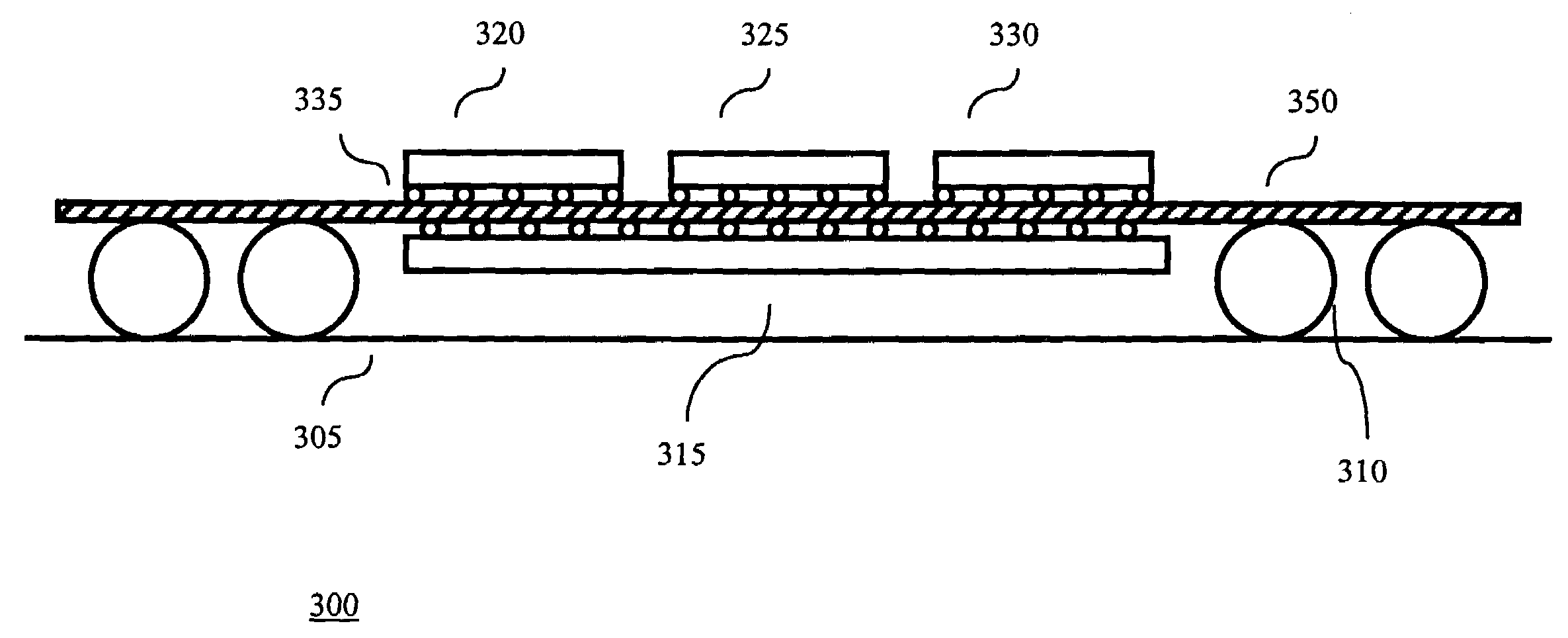
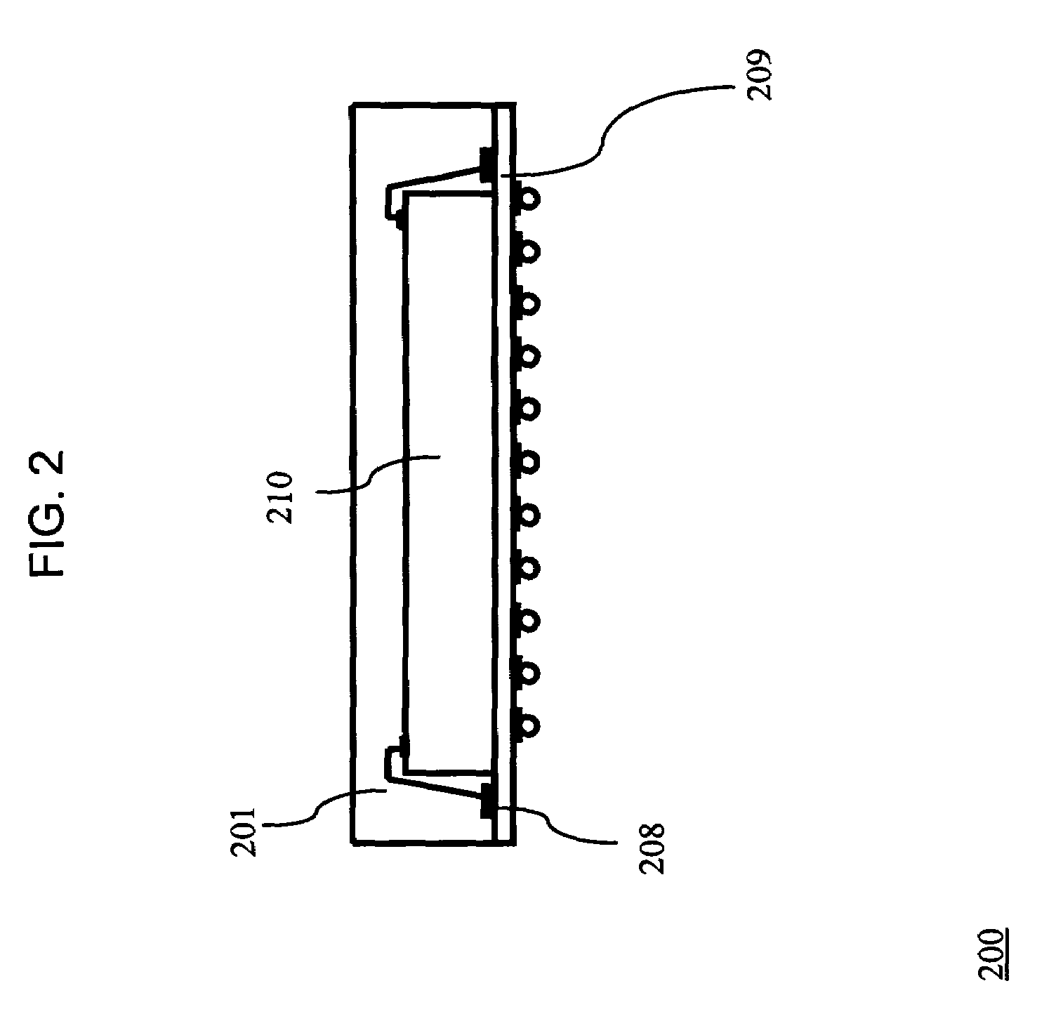
[0024]A packaged semiconductor chip 100 is illustrated in FIG. 1. As used in this disclosure, the term “packaged semiconductor chip” refers to a unit including both the actual semiconductor element or “bare die” itself, and one or more components or layers which cover at least one surface or edge of the bare die. Typically, but not necessarily, a packaged chip has electrical connection elements distinct from the contacts of the bare die itself. As used in this disclosure, the term “standard packaged chip” refers to a packaged chip having electrical connection elements (whether or not distinct from the contacts of the bare die) disposed in a pattern conforming to an official or unofficial standard applicable to packaged chips. Most preferably, the standard packaged chips conform to a standard applicable to packaged chips intended for mounting to circuit boards. Illustratively, packaged semiconductor chip 100 is a Tessera® Compliant Chip as known in the art. However, other forms of pa...


PUM


Abstract

An ultra thin system-in-a-package (SIP) with independent test and repair capability comprises an interposer having arranged on a top surface and a bottom surface thereof a number of packaged semiconductor chips mounted via solder bumps in accordance with a Land Grid Array (LGA) format and wherein no underfill is used on the SIP.

Description


Claims


Application Information

Patent Timeline
Owner TESSERA INC
Why Eureka
Try Eureka