

Three-dimensional integrated CMOS-MEMS device and process for making the same
- Summary
- Abstract
- Description
- Claims
- Application Information
AI Technical Summary
Problems solved by technology
Method used
Image

Examples
Embodiment Construction
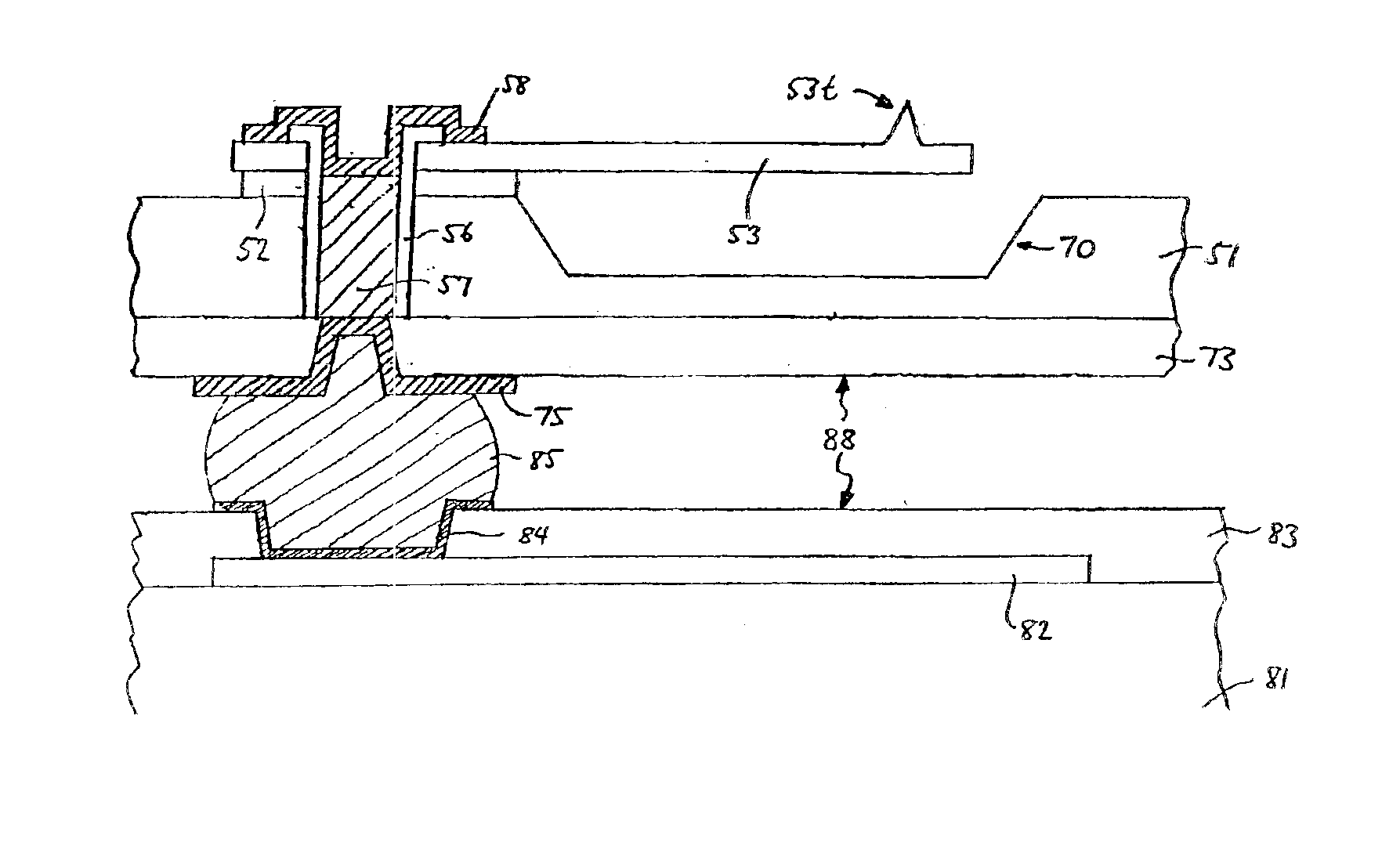
[0035]FIG. 3 illustrates an embodiment of the invention wherein a memory storage device includes 3-dimensional integration of a MEMS chip 1 and a CMOS chip 2, and where the connections between the chips are made using C4 technology. The MEMS chip has an array of cantilevers 10 aligned to an array of C4 solder bumps 30 on the CMOS chip. The cantilevers 10 on the MEMS chip make contact with the storage medium 12. Movement of the cantilevers is controlled by the CMOS chip; connection between an individual cantilever and the CMOS chip is through an electrical pathway which includes interconnect 15 through the MEMS chip, pad 33 formed on a polyimide layer 31 on the backside of the MEMS chip, and the C4 solder bump 30. (The solder bump is connected to a pad, not shown, formed on a polyimide layer 32 on the CMOS chip 2.)
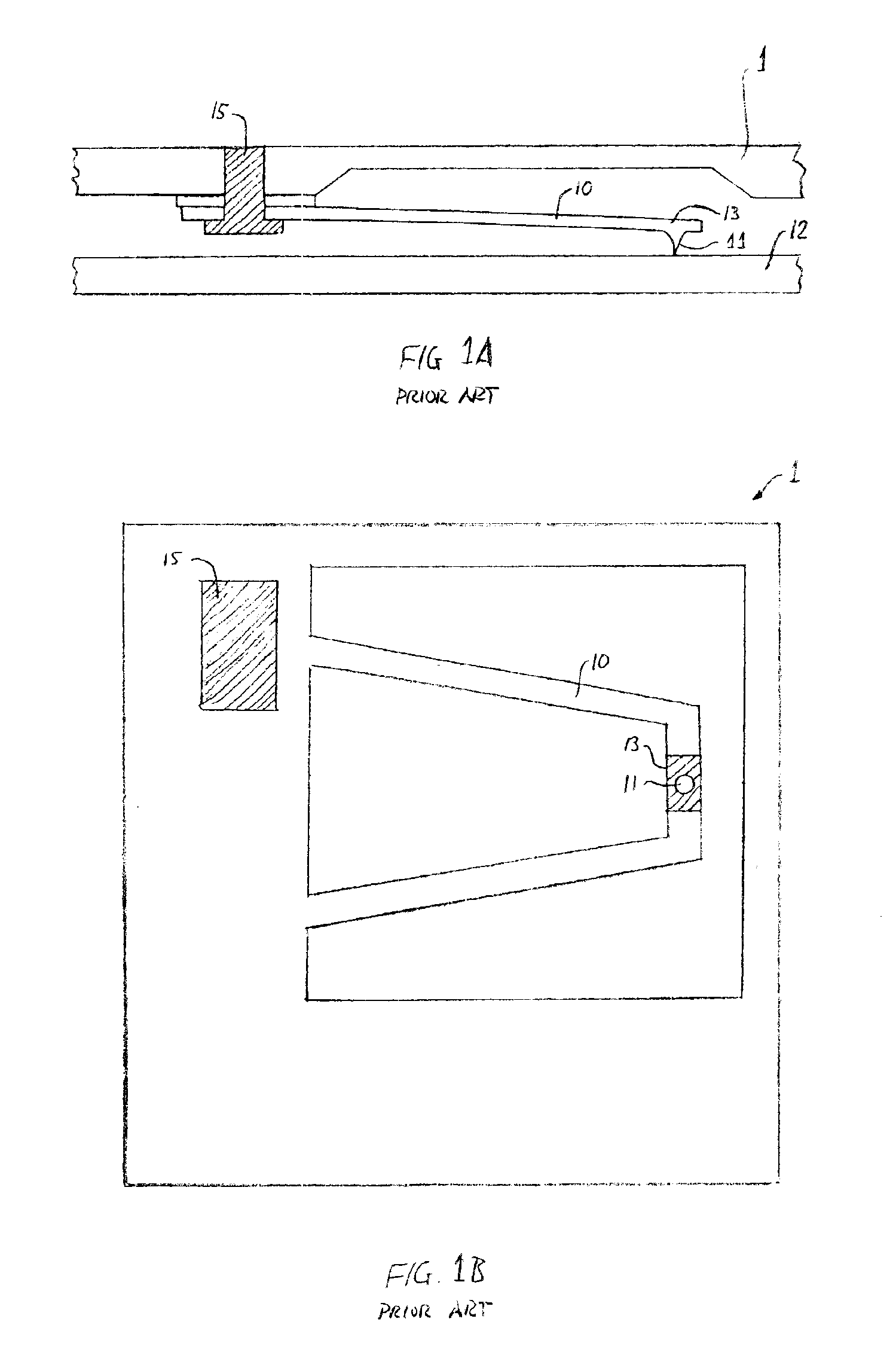
[0036]FIG. 4 illustrates another embodiment of the invention, wherein a memory storage device is fabricated by integrating a MEMS chip 1 and a CMOS chip 2 using vertical st...
PUM
| Property | Measurement | Unit |
|---|---|---|
| Electrical conductor | aaaaa | aaaaa |
| Height | aaaaa | aaaaa |
| Transparency | aaaaa | aaaaa |
Abstract
Description
Claims
Application Information