Method for improved process latitude by elongated via integration

a technology of integration and process latitude, applied in the direction of semiconductor devices, semiconductor/solid-state device details, electrical devices, etc., can solve the problem that the printing latitude is one of the most difficult problems

Active Publication Date: 2006-07-04
ELPIS TECH INC
View PDF13 Cites 21 Cited by
  • Summary
  • Abstract
  • Description
  • Claims
  • Application Information

AI Technical Summary

Problems solved by technology

Traditionally, the via levels are one of the most challenging to print with a high process latitude.

Method used


Image

  • Method for improved process latitude by elongated via integration
  • Method for improved process latitude by elongated via integration
  • Method for improved process latitude by elongated via integration

Examples


Embodiment Construction

[0025]In order to facilitate a further understanding of the present invention, reference will be made to the Figures.

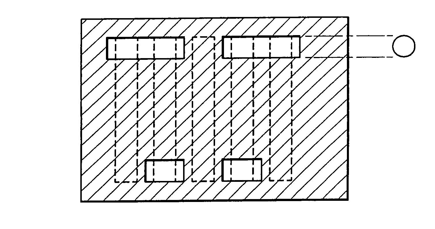
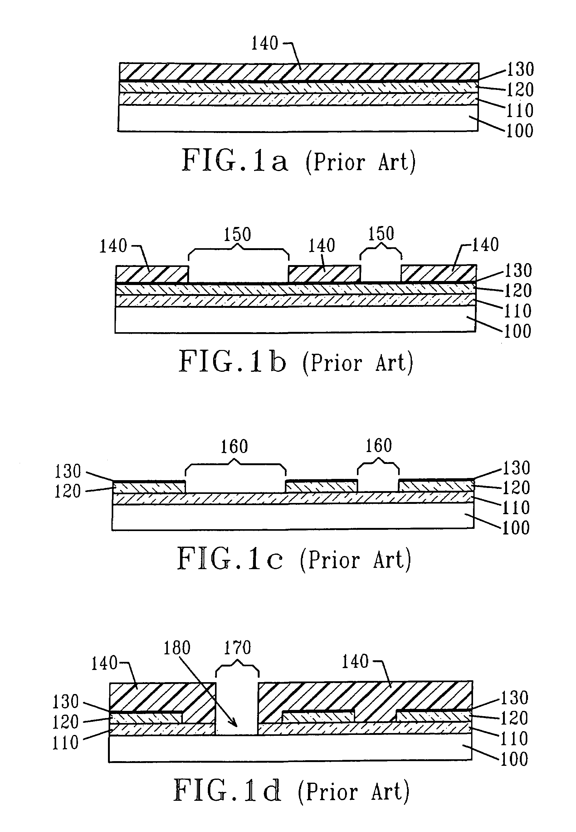
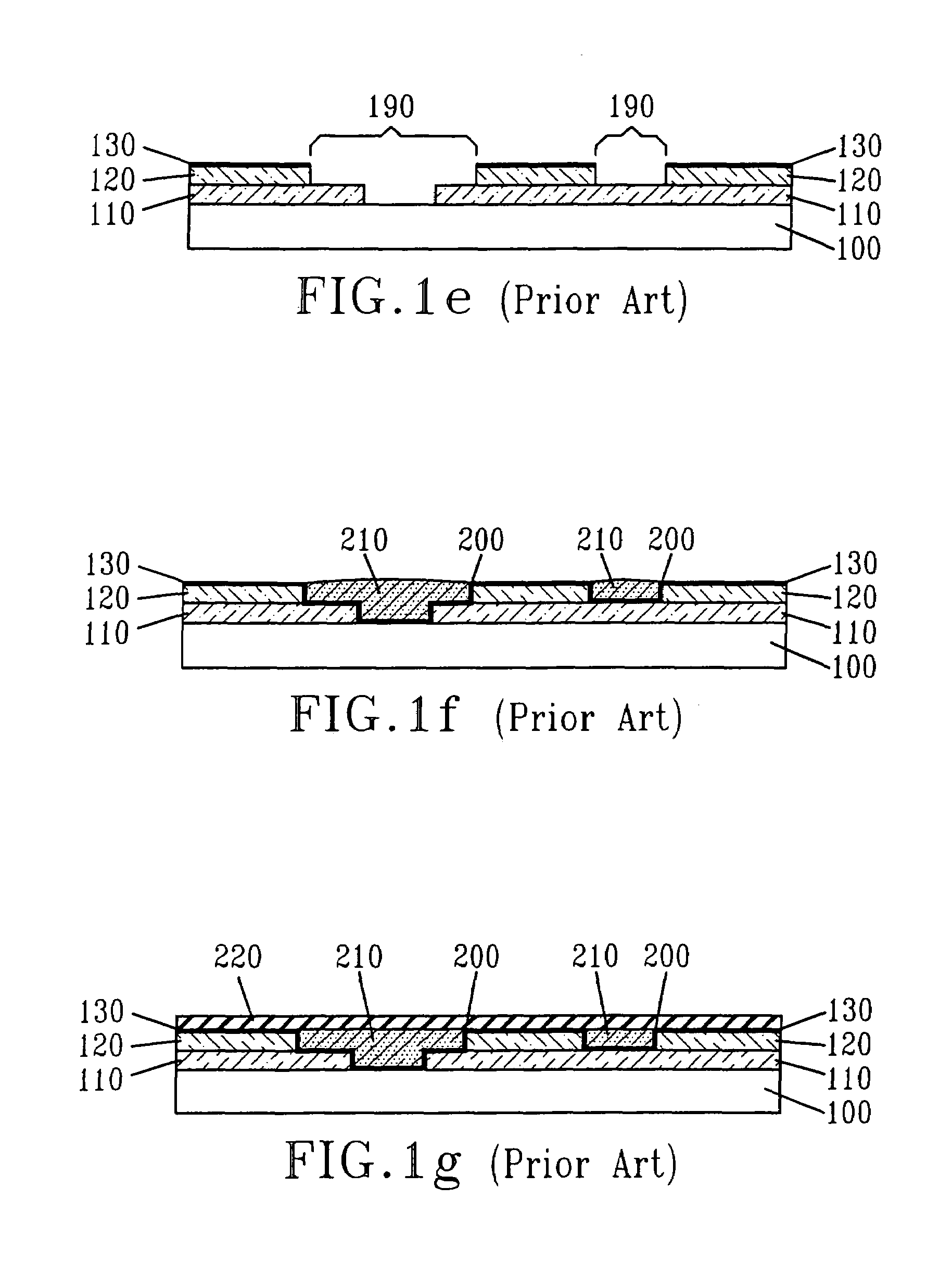
[0026]Reference to FIG. 2a shows coating a substrate 10 with a via-level dielectric 11 and a via-level mask 12. Typical insulating or dielectric material 11 include silicon dioxide (SiO2) phosphosilicate glass (PSG), boron doped PSG (BDPSG) or tetraethylorthosilicate (TEOS), and more typically low-k dielectrics having a dielectric constant of less than 3.9 such as SILK (available from Dow Chemical), SiCH (available from AMAT under the trade designation BLOK), SiCOH (available from Novellus under the trade designation Coral, from AMAT under the trade designation Black Diamond and from ASM under the trade designation Auora), SiCHN (available from IBM under the trade designation N Blok), CVD carbon-doped oxide, porous CVD carbon-doped oxide, porous and non-porous organo silicates, porous and non-porous organic spin-on polymers.

[0027]The via-level mask 12 is typically a h...


PUM


Abstract

Interconnect dual damascene structure are fabricated by depositing on a layer of at least one dielectric, a mask forming layer for providing the via-level mask layer of the dual damascene structures; creating an elongated via pattern in the via-level mask layer; depositing a layer of line-level dielectric and creating a line pattern through the layer of line-level dielectric, and transferring the line pattern through the projected intersection of the elongated via-level pattern and of the line-level pattern thereby generating an aligned dual damascene structure. A conductive liner layer is deposited in the dual damascene structure followed by filling the dual damascene structure with a conductive fill metal to form a set of metal lines. The metal and liner layers are planarized.

Description

FIELD OF THE INVENTION[0001]The present invention pertains to the process of producing intralayer and interlayer structures in Very-Large Scale Integrated (VLSI) and Ultra-Large Scale Integrated (ULSI) devices and high performance packaging. More particularly, the present invention relates to fabricating interconnect dual damascene structures.BACKGROUND OF THE INVENTION[0002]The fabrication of Very-Large Scale Integrated (VLSI) or Ultra-Large Scale Integrated circuit (ULSI) requires metallic wiring that connects individual devices in a semiconductor chip, to one another. One method of creating this wiring network on such a small scale is the dual damascene (DD) process schematically shown in FIG. 1. In the standard DD process, an interlayer dielectric (ILD), shown as two layers 110, 120 is coated on the substrate 100, FIG. 1a. The via level dielectric 110 and the line level dielectric 120 are shown separately for clarity of the process flow description. In general, these two layers ...

Claims


Application Information

Patent Timeline
Patent Type & Authority Patents(United States)
IPC IPC(8): H01L21/4763H01L21/44H01L23/48H01L23/52
CPCH01L21/76807H01L21/76835H01L21/76829H01L21/7681
Inventor COLBURN, MATTHEW E.
Owner ELPIS TECH INC
Why Eureka
Try Eureka