Pattern inspecting apparatus and method

a technology of pattern repetition and apparatus, applied in the field of pattern repetition pattern inspection apparatus and method, can solve the problems of not being able to detect defects occurring over two or more repetition cycles, and needing a relatively large error allowance, and achieve the effect of reducing pattern area and reducing pattern repetition random area

Active Publication Date: 2006-09-26
DAINIPPON SCREEN MTG CO LTD
View PDF14 Cites 12 Cited by
  • Summary
  • Abstract
  • Description
  • Claims
  • Application Information

AI Technical Summary

Benefits of technology

[0021]With this pattern inspecting method, the patterns on each chip are photographed and displayed in enlargement on the display device. These patterns are used in setting a repetitive pattern area having repetitive patterns formed therein, and a random pattern area having random patterns formed therein. In this way, the repetitive pattern area and random pattern area are set with ease.

Problems solved by technology

The chip comparing inspection compares and inspects patterns arranged in two relatively remote locations on a semiconductor wafer, and therefore needs a relatively large error allowance.
This cell comparing inspection provides highly accurate results for minute defects formed in repetitive patterns, but cannot detect defects occurring over two or more cycles of pattern repetition.
Such a problem is a phenomenon occurring also with the pattern defect inspecting method described in U.S. Pat. No. 2,976,550 noted above.
In time of cell comparing inspection, the relatively large defect present over two or more cycles of pattern repetition will result in a finding that no defect is present.

Method used


Image

  • Pattern inspecting apparatus and method
  • Pattern inspecting apparatus and method
  • Pattern inspecting apparatus and method

Examples


Embodiment Construction

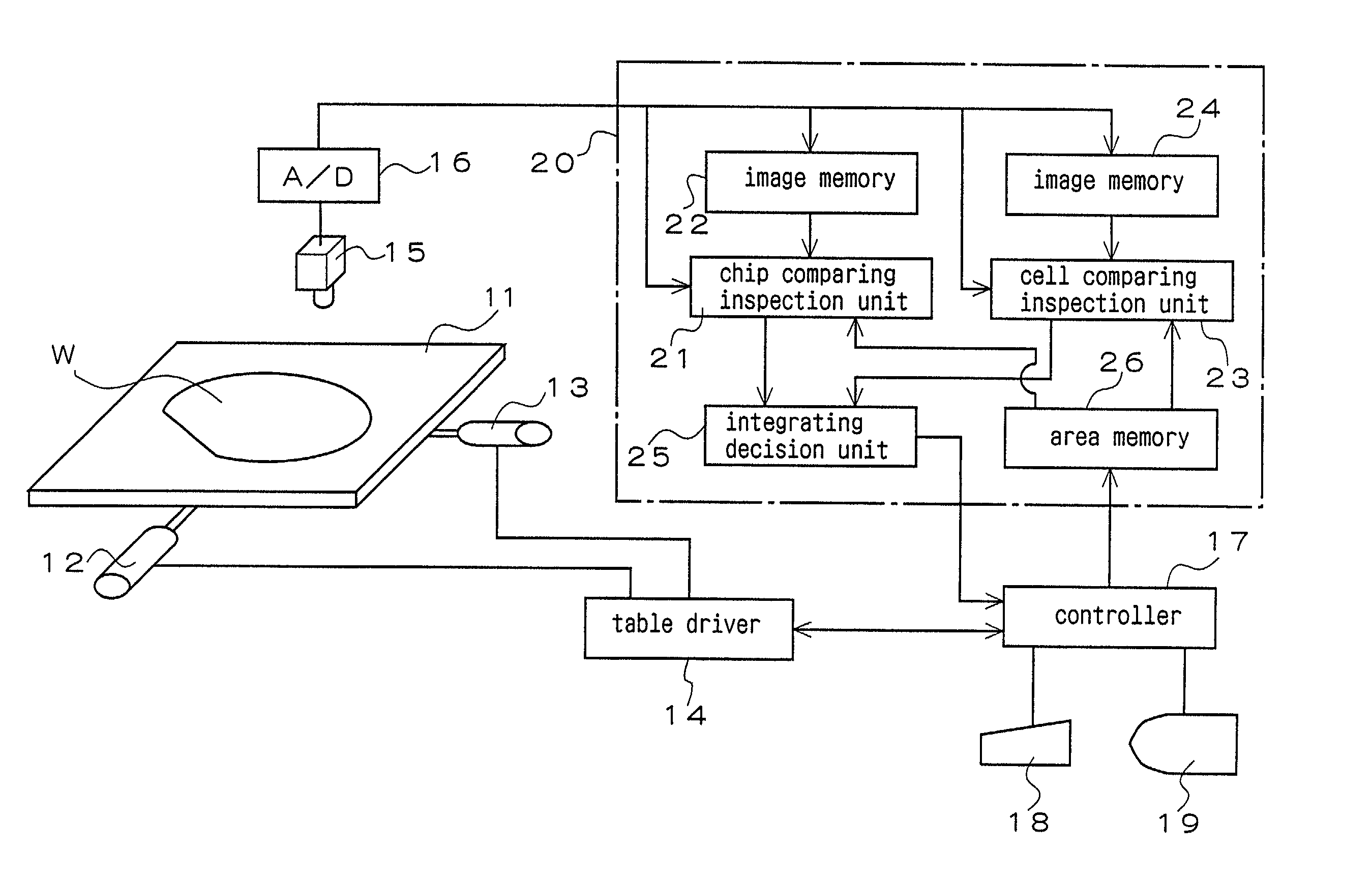
[0040]Embodiments of the present invention will be described hereinafter with reference to the drawings. FIG. 1 is a schematic view of a pattern inspecting apparatus according to the invention.

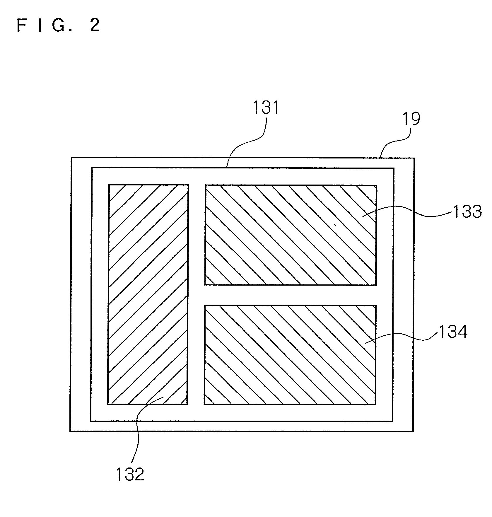
[0041]This pattern inspecting apparatus includes a substrate support table 11 for supporting a substrate, e.g. semiconductor wafer W, an actuator 12 for moving the substrate support table 11 in X-direction, an actuator 13 for moving the substrate support table 11 in Y-direction, a table driver 14 for driving the substrate support table 11 through the actuators 12 and 13, a camera 15 for photographing chips formed on the wafer W supported by the substrate support table 11, an image processor 20 to be described hereinafter, and a controller 17 for controlling the entire pattern inspecting apparatus. The controller 17 has, connected thereto, a keyboard 18 acting as an area setting device in time of area setting as described hereinafter, and a CRT 19 acting as an enlarged image display device.

[004...


PUM

PropertyMeasurementUnit
area memoryaaaaaaaaaa
defectaaaaaaaaaa
pattern defect inspectingaaaaaaaaaa

Abstract

A pattern inspecting apparatus includes a substrate support table, a table driver for driving the substrate support table through actuators, a camera, an image processor, and a controller connected to a keyboard and a CRT. The image processor has a chip comparing inspection unit for executing a chip comparing inspection, a cell comparing inspection unit for executing a cell comparing inspection, an image memory, an integrating decision unit for integrating results of inspection by the chip comparing inspection unit and results of inspection by the cell comparing inspection unit and making a final decision as to the presence of a defect, and an area memory.

Description

BACKGROUND OF THE INVENTION[0001]1. Field of the Invention[0002]The present invention relates to a pattern inspecting apparatus and method for inspecting patterns in numerous chips formed on substrates such as semiconductor wafers.[0003]2. Description of the Related Art[0004]Numerous chips formed on a semiconductor wafer include repetitive pattern areas having the same pattern formed repeatedly, such as charge storage portions of memory, and random pattern areas having other patterns formed therein. In inspecting such patterns in the chips, different inspecting methods are used for the repetitive pattern areas and random pattern areas.[0005]That is, for the random pattern areas, a chip comparing inspection is employed to detect pattern defects by comparing corresponding patterns in a plurality of adjoining or adjacent chips. This chip comparing inspection is an inspecting method also called a die comparing inspection or random comparing inspection. The chip comparing inspection comp...

Claims


Application Information

Patent Timeline
Patent Type & Authority Patents(United States)
IPC IPC(8): G06K9/00G01N21/956G06T7/00G06T7/40G06T7/60
CPCG01N21/95607G06T7/0002G06T7/001G06T2207/30148G06T7/49G06T7/68
Inventor ONISHI, HIROYUKI
Owner DAINIPPON SCREEN MTG CO LTD
Why Eureka
Try Eureka