Stacked BGA packages

a technology of stacked bga and stacked bga, which is applied in the field of stacked bga (ball grid array) package, can solve the problems of reducing yield, and increasing the cost of chip stacked devices that are discarded, so as to achieve the effect of increasing the density of packaging

Inactive Publication Date: 2006-10-10
SAMSUNG ELECTRONICS CO LTD
View PDF14 Cites 172 Cited by
  • Summary
  • Abstract
  • Description
  • Claims
  • Application Information

AI Technical Summary

Benefits of technology

[0012]In another exemplary embodiment according to the present invention, a multiple stacked BGA package is provided wherein two or more double stacked BGA packages according to the present invention are, in turn, stacked. An exemplary multiple stacked BGA package according to the invention includes a first double stacked BGA package disposed below a second double stacked BGA package with the solder balls arranged on the lower BGA package of the second double stacked BGA package serving to connect the second double stacked BGA package to connection regions provided on the substrate of the upper BGA package of the first double stacked BGA package. These connection regions may be contact terminals disposed on the substrate of the upper BGA package of the first double stacked BGA package and connected to the chip incorporated in in the upper BGA package of the first double stacked BGA package. Both the double and multiple stacked BGA package manufactured according to the invention have a peripheral size approaching that of the incorporated semiconductor chips, thereby allowing the packaging density to be increased.

Problems solved by technology

Because typically only the basic electrical characteristics and functionality of the chips are tested before packaging, chip stacked devices are more likely to incorporate one or more chips having incomplete functionality and / or inadequate performance.
This result is problematic because the packaging process itself may be relatively expensive compared to the chip cost and good chips will likely be discarded along with the underperforming chip(s), thereby reducing the yield and increasing the cost when chip stacked devices are discarded.
The BGA packages included in this conventional stacked BGA package structure are larger than the incorporated semiconductor chips 115, 125, making it difficult to incorporate or adapt such BGA packages into package stacked devices that more closely approximate a chip scale package (CSP) sizing.
In addition, the ability to reduce the height of the conventional stacked BGA package device illustrated in FIG. 1 is hampered by the size of the solder balls 122 required to maintain a gap 127 or separation distance between the lower and upper BGA packages 110 and 120.

Method used


Image

  • Stacked BGA packages
  • Stacked BGA packages
  • Stacked BGA packages

Examples


first embodiment

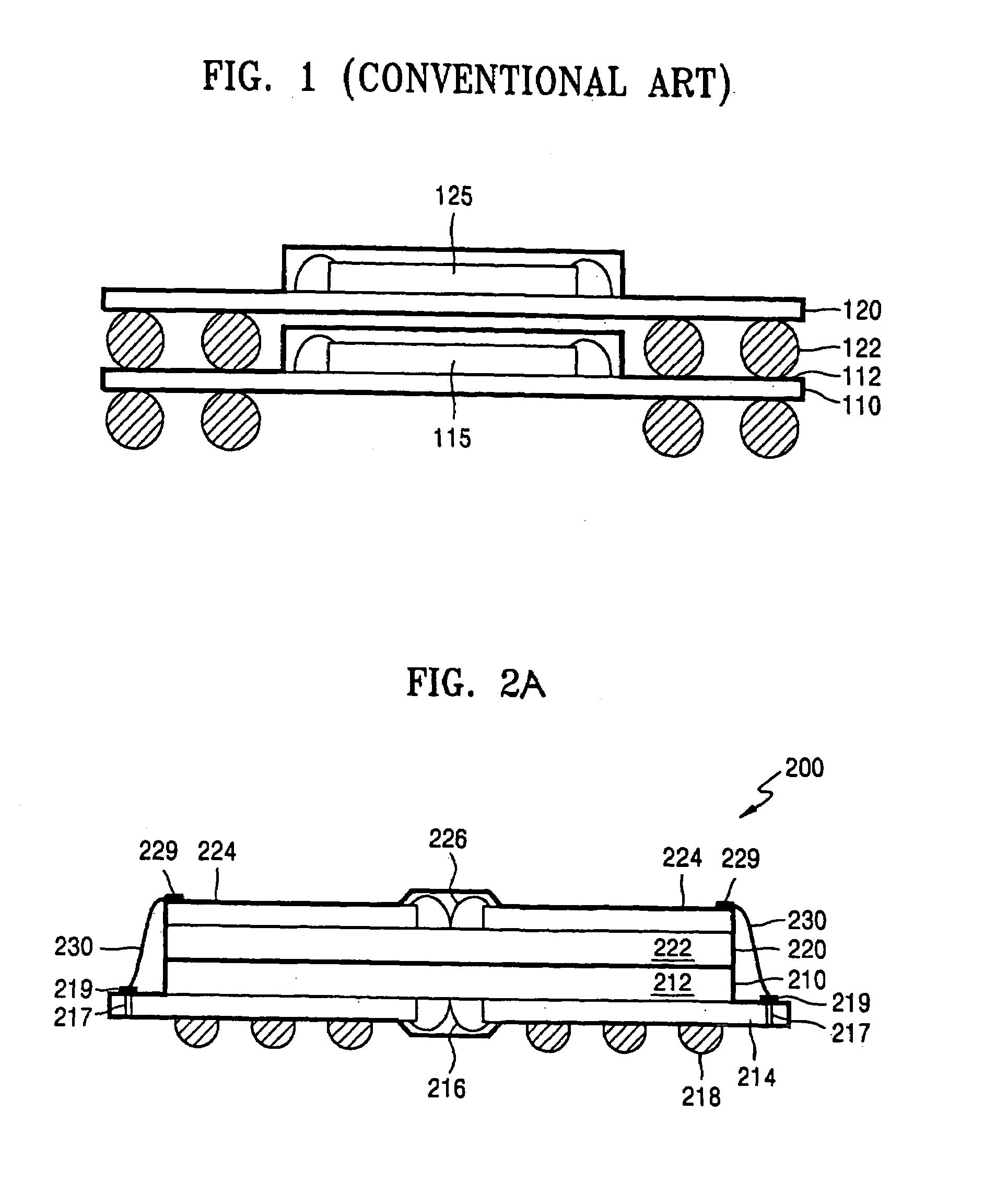
[0021]FIG. 2A is a cross-sectional view illustrating a double stacked BGA package according to the present invention. The double stacked BGA package 200 has a stacked structure in which lower and upper stacked BGA packages 210 and 220 are attached to each other. More specifically, an adhesive composition is provided between the back surfaces (also referred to as the backside surfaces) of the semiconductor chips 212, 222 for attaching the two chips together, thereby also attaching the lower and upper BGA packages 210, 220 together in a package stacked arrangement. In this arrangement the active surfaces, i.e., those surfaces on which the semiconductor device circuitry is provided, of both semiconductor chips are oriented toward the exterior surfaces of the stacked package device. The adhesive composition may form an adhesive layer.

[0022]The semiconductor chip 212 incorporated in the lower BGA package 210 may be electrically connected to the substrate 214 through bonding wires 216. Si...

second embodiment

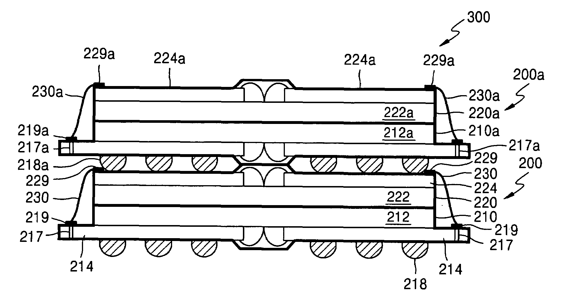
[0026]FIG. 3 is a view illustrating a multiple stacked BGA package 300 according to the present invention. The multiple stacked BGA package 300 is constructed by stacking two double stacked BGA packages 200, 200a, both of which, in this instance, each generally correspond to the stacked BGA package 200 previously described and as illustrated in FIG. 2A. The lower double stacked BGA package 200 is illustrated with the same reference numerals as the double stacked BGA package 200 of FIG. 2A while the reference numerals associated with the upper double stacked BGA package 200a include a corresponding “a” suffix.

[0027]In the multiple stacked BGA package 300, the chips 212 and 222 of the lower double stacked BGA package 200, which are connected through the solder balls 218, the through holes 217, the contact terminals 219 of the lower BGA package 210, the flexible substrate 230, and the contact terminals 229 of the upper BGA package 220, are electrically connected to the chips 212a and 2...


PUM


Abstract

Provided are double stacked and multiple stacked BGA packages in which two or more BGA packages are stacked to increase the packaging density. Each of the individual BGA packages included in the stacked BGA packages includes at least one semiconductor chip and a substrate on which the chip is mounted with the substrate(s) being sized to be approximately the same size or, in some instances, slightly larger than the semiconductor chip(s) mounted thereon. A plurality of external contact terminals are provided on each of the substrates, with the corresponding external contact terminals of the multiple BGA packages being electrically connected using a flexible substrate.

Description

CROSS-REFERENCE TO RELATED APPLICATION[0001]This application claims the priority of Korean Patent Application No. 2003-80079, which was filed on Nov. 13, 2003, in the Korean Intellectual Property Office, the disclosure of which is incorporated herein in its entirety by reference.BACKGROUND OF THE INVENTION[0002]1. Field of the Invention[0003]The present invention relates to a semiconductor device, and more particularly, to a stacked BGA (ball grid array) package capable of increasing packaging density per area.[0004]2. Description of the Related Art[0005]As semiconductor technologies have become advanced, more highly integrated and higher performing semiconductor devices have been developed. One of the methods developed for increasing the capability of a semiconductor device is a method of stacking multiple chips or packages in a single device. These semiconductor stacking methods allow semiconductor device package density to be increased even in instances in which the sizes of the ...

Claims


Application Information

Patent Timeline
Patent Type & Authority Patents(United States)
IPC IPC(8): H01L23/40H01L23/02H01L23/52H01L29/40H01L25/18H01L23/12H01L23/538H01L25/065H01L25/07H01L25/10
CPCH01L23/5387H01L25/105H01L2224/06136H01L2224/48091H01L2224/4824H01L2225/06558H01L2924/15311H01L2924/15331H01L2924/16152H01L2924/19107H01L24/48H01L2225/1023H01L2225/1041H01L2225/1058H01L2224/73265H01L2224/32145H01L2924/00014H01L2224/45099H01L2224/45015H01L2924/207H01L23/12
Inventor KIM, JUNG-JIN
Owner SAMSUNG ELECTRONICS CO LTD
Why Eureka
Try Eureka