High voltage semiconductor device having high breakdown voltage and method of fabricating the same

Inactive Publication Date: 2006-10-31
SEMICON COMPONENTS IND LLC
View PDF5 Cites 2 Cited by
  • Summary
  • Abstract
  • Description
  • Claims
  • Application Information

AI Technical Summary

Benefits of technology

[0010]To solve the above problems, it is a first object of the present invention to provide a high voltage semiconductor device having a high breakdown voltage and a narrow junction termination.
[0011]It is a second object of the present invention to provide a method of fabricating the high voltage semiconductor device.
[0012]Accordingly, to achieve the above first object, there is provided a high voltage semiconductor device. The high voltage semiconductor device includes: a high concentration collector area of a first conductive type; a low concentration collector area of a first conductive type formed on the high concentration collector area; a base area of a second conductive type formed on the low concentration collector area and having a trench which penetrates the low concentration collector area in a vertical direction at the edge of the trench; a high concentration emitter area of a first conductive type formed on a predetermined upper surface of the base area; and an emitter electrode, a base electrode, and a collector electrode isolated from one another and connected to the emit

Problems solved by technology

However, these methods all demand a wide junction termination area to obtain a high breakdown voltage.

Method used


Image

  • High voltage semiconductor device having high breakdown voltage and method of fabricating the same
  • High voltage semiconductor device having high breakdown voltage and method of fabricating the same
  • High voltage semiconductor device having high breakdown voltage and method of fabricating the same

Examples


Embodiment Construction

[0020]Hereinafter, preferred embodiments of the present invention will be described in detail with reference to the attached drawings. However, the embodiments of the present invention can be modified into various other forms, and the scope of the present invention must not be interpreted as being restricted to the embodiments. The embodiments are provided to more completely explain the present invention to those skilled in the art. In the drawings, the thicknesses of layers or regions are exaggerated for clarity. Like reference numerals in the drawings denote the same members. Also, when it is written that a layer is formed “on” another layer or a substrate, the layer can be formed directly on the other layer or the substrate, or other layers can intervene therebetween.

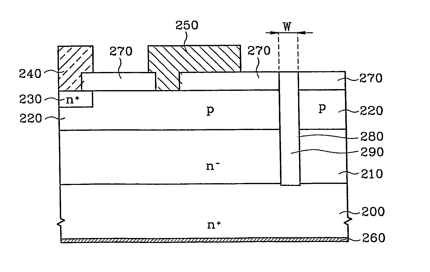
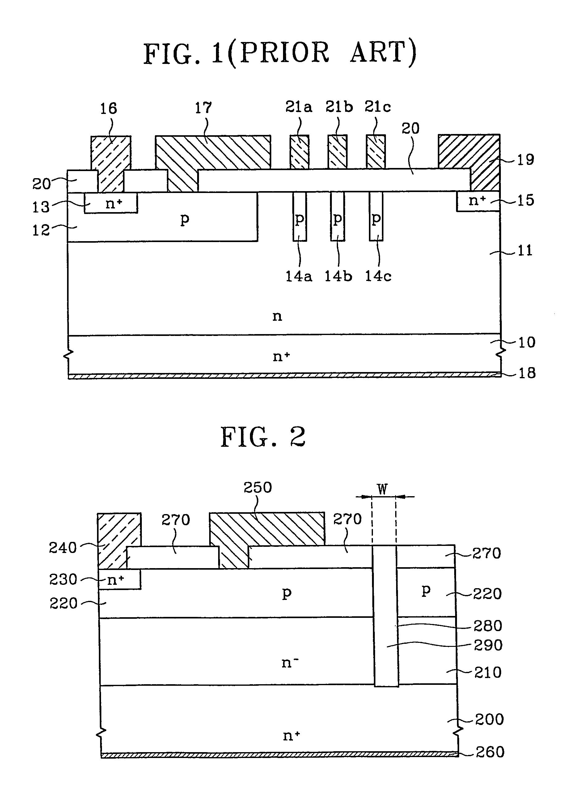
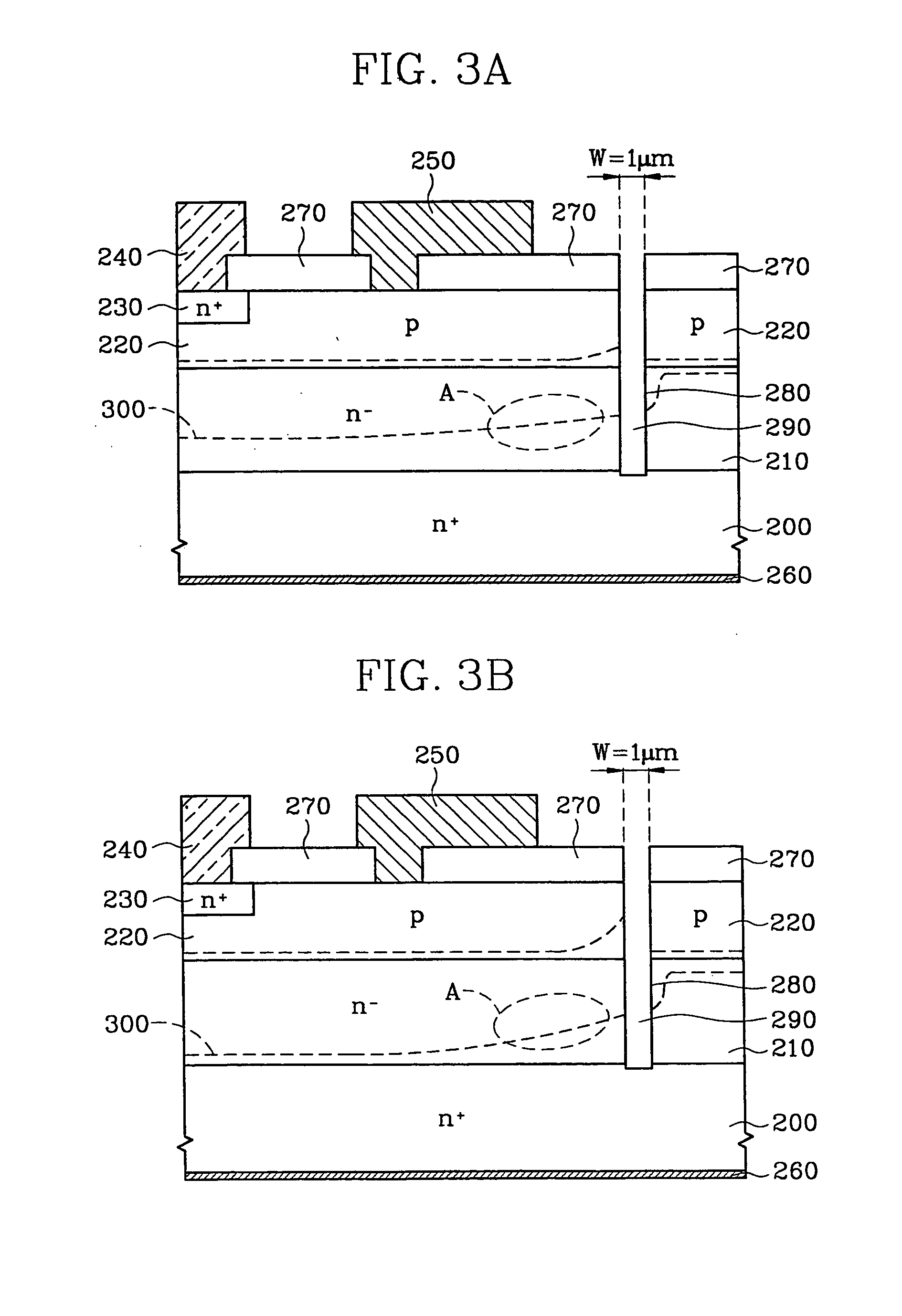
[0021]FIG. 2 is a cross-sectional view of a junction termination of a high voltage semiconductor device according to the present invention. Referring to FIG. 2, a low concentration first conductive type, e.g., an n−-...


PUM


Abstract

A high voltage semiconductor device, including: a high concentration collector area of a first conductive type; a low concentration collector area of a first conductive type formed on the high concentration collector area; a base area of a second conductive type formed on the low concentration collector area and having a trench perforating the low concentration collector area in a vertical direction at the edge of the trench; a high concentration emitter area of a first conductive type formed on a predetermined upper surface of the base area; and an emitter electrode, a base electrode, and a collector electrode isolated from one another and connected to the emitter area, the base area, and the collector area, respectively. High breakdown voltage can be obtained with a narrow junction termination area due to the trench.

Description

CROSS REFERENCE TO RELATED APPLICATION[0001]This application is a continuation of U.S. application Ser. No. 10 / 024,475, filed Dec. 21, 2001, now abandoned.BACKGROUND OF THE INVENTION[0002]1. Field of the Invention[0003]The present invention relates to a high voltage semiconductor device and a method of fabricating the same, and more particularly, to a high voltage semiconductor device having a high breakdown voltage and a method of fabricating the same.[0004]2. Description of the Related Art[0005]A strong electric field is generated at the inside or edge of a high voltage device, which reduces the breakdown voltage of the high voltage device. A representative method of preventing a strong electric field from being generated at the edge of the high voltage device is to use a floating field ring (also called a field limiting ring). The floating field ring, which is formed around a main junction without any electric contact, reduces the concentration of an electric field at a cylindric...

Claims


Application Information

Patent Timeline
IPC IPC(8): H01L31/119H01L29/70H01L21/331H01L29/06H01L29/732
CPCH01L29/0661H01L29/66295H01L29/732H01L29/70
Inventor PARK, CHAN-HO
Owner SEMICON COMPONENTS IND LLC
Why Eureka
Try Eureka