Semiconductor device and method of manufacturing the same

Active Publication Date: 2019-11-07
HYUNDAI MOTOR CO LTD +1
View PDF9 Cites 0 Cited by
  • Summary
  • Abstract
  • Description
  • Claims
  • Application Information

AI Technical Summary

Benefits of technology

[0007]Various aspects of the present invention are directed to providing a s

Problems solved by technology

In a case of a SiC PiN diode, aspects that are suitable for a SiC diode element exist due t

Method used


Image

  • Semiconductor device and method of manufacturing the same
  • Semiconductor device and method of manufacturing the same
  • Semiconductor device and method of manufacturing the same

Examples


Embodiment Construction

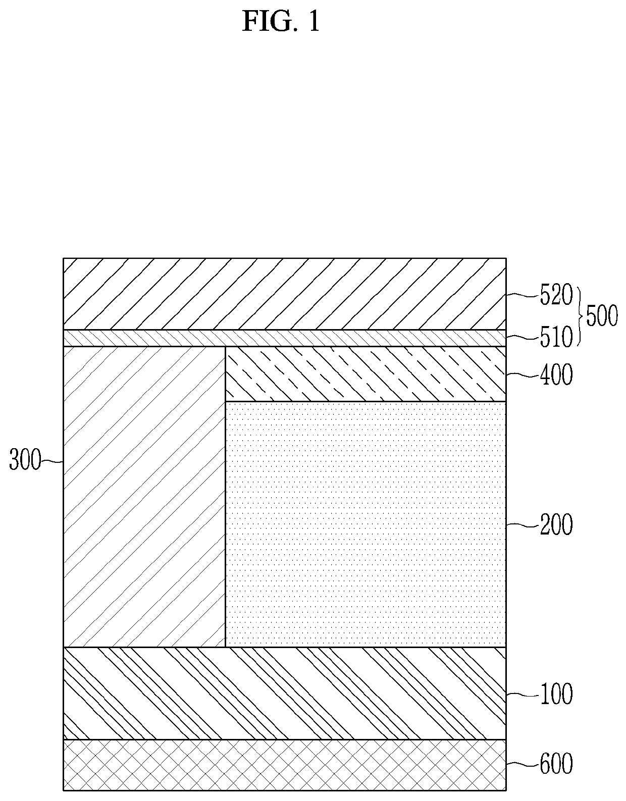
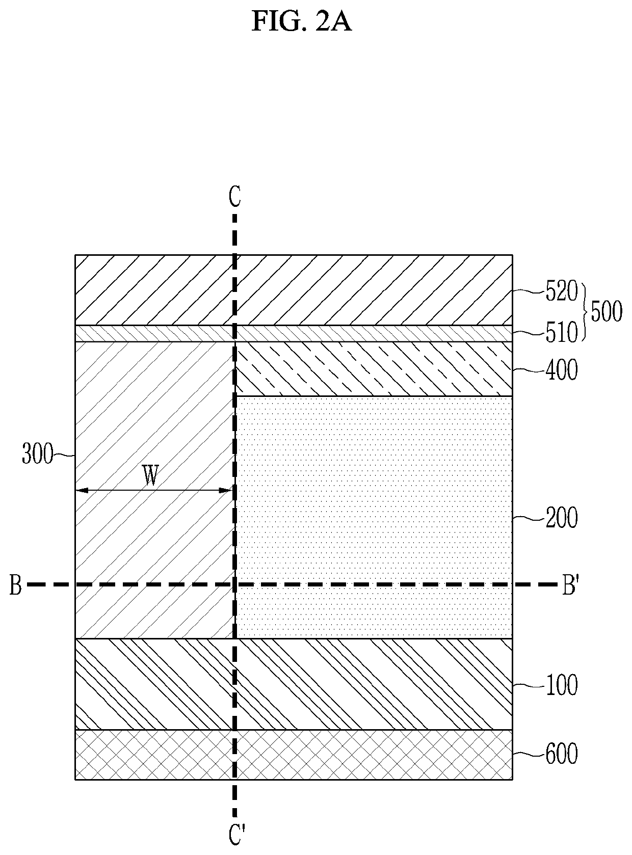
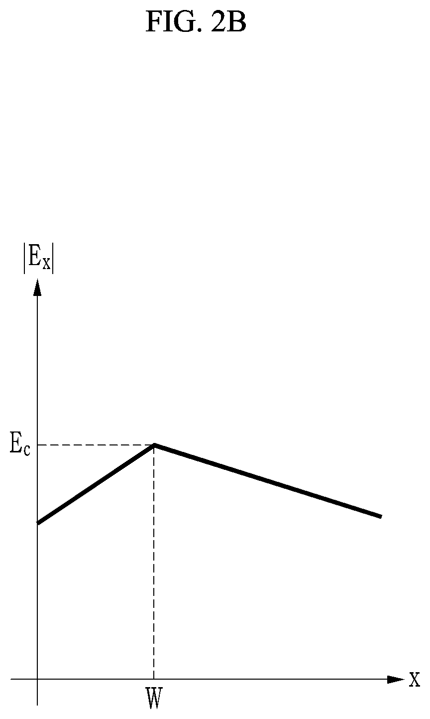
[0030]Reference will now be made in detail to various embodiments of the present invention(s), examples of which are illustrated in the accompanying drawings and described below. While the invention(s) will be described in conjunction with exemplary embodiments, it will be understood that the present description is not intended to limit the invention(s) to those exemplary embodiments. On the other hand, the invention(s) is / are intended to cover not only the exemplary embodiments, but also various alternatives, modifications, equivalents and other embodiments, which may be included within the spirit and scope of the invention as defined by the appended claims.

[0031]Hereinafter, various exemplary embodiments of the present invention will be described in detail with reference to the accompanying drawings. As those skilled in the art would realize, the described embodiments may be modified in various different ways, all without departing from the spirit or scope of the present invention...


PUM


Abstract

A semiconductor device may include: an n type of layer disposed on a first surface of a substrate; a p+ type of region disposed on the first surface of the substrate; a p− type of region disposed at a top portion of the n type of layer; a first electrode disposed on the p+ type of region and the p− type of region; and a second electrode disposed on a second surface of the substrate, wherein the side surface of the p+ type of region and the side surface of the n type of layer are in contact, and the thickness of the p+ type of region is the same as the thickness of the n type of layer and the thickness of the p− type of region.

Description

CROSS-REFERENCE TO RELATED APPLICATION[0001]The present application claims priority to Korean Patent Application No. 10-2018-0051816 filed on May 4, 2018, the entire contents of which is incorporated herein for all purposes by this reference.BACKGROUND OF THE INVENTIONField of the Invention[0002]The present invention relates to a semiconductor device including a silicon carbide (SiC), and a manufacturing method thereof.Description of Related Art[0003]In accordance with trends towards large size and large capacity of an appliance in recent years, a necessity of a power semiconductor device having a high breakdown voltage, a high current, and a high speed switching characteristic comes to the front. A silicon carbide (SiC) power device that has been pointed out as the only device that can satisfy the above-described characteristic due to its superior characteristics with respect to a conventional silicon (Si) device is currently being actively researched and is in an early stage of ma...

Claims


Application Information

Patent Timeline
IPC IPC(8): H01L29/872H01L29/06H01L29/417H01L29/16H01L21/02H01L21/04H01L29/66H01L29/36
CPCH01L29/872H01L29/1608H01L21/0475H01L21/02529H01L29/66143H01L29/36H01L21/046H01L29/6606H01L29/0684H01L21/0485H01L21/0495H01L21/02634H01L21/02378H01L29/417H01L29/0603H01L29/0634
Inventor CHUN, DAE HWANJOO, NACKYONG
Owner HYUNDAI MOTOR CO LTD
Why Eureka
Try Eureka