Schottky diode with high breakdown voltage and surge current capability using double p-type epitaxial layers

Inactive Publication Date: 2020-01-23
AZ POWER INC
View PDF0 Cites 1 Cited by
  • Summary
  • Abstract
  • Description
  • Claims
  • Application Information

AI Technical Summary

Benefits of technology

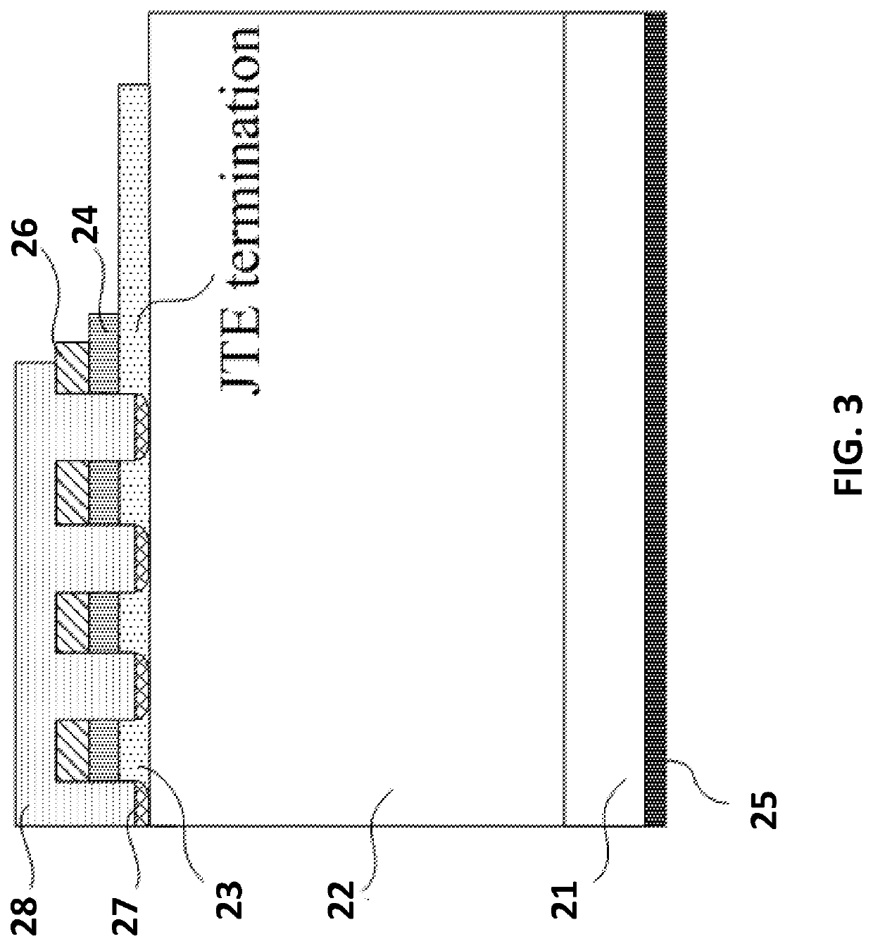
This patent introduces a method for making a Schottky barrier diode with high breakdown voltage and surge current capability using double P-type epitaxial semiconductor layers. This method allows for a low-temperature production process, reducing the need for expensive manufacturing equipment and processes. The end portion of the diode is formed into a junction termination extension (JTE) structure, which includes an optimized impurity concentration and width in the remaining P-type epitaxial layer to achieve high breakdown voltage. The present invention also has an advantage of high accuracy and controllability of impurity concentration, important in the implantation process. Overall, this method results in a more efficient and cost-effective production of Schottky barrier diodes.

Problems solved by technology

For a pure Schottky barrier diode, a major problem is that it's surge current capability is low when compared with PN junction diode.
However, ion implantation can damage the high-concentration impurity region.
Furthermore, a high temperature process is needed for the conventional JBS / MPS diode, which is not compatible with the manufacturing process, and expensive production installations and production process are usually required for manufacturing the JBS / MPS diode.

Method used


Image

  • Schottky diode with high breakdown voltage and surge current capability using double p-type epitaxial layers
  • Schottky diode with high breakdown voltage and surge current capability using double p-type epitaxial layers
  • Schottky diode with high breakdown voltage and surge current capability using double p-type epitaxial layers

Examples


Embodiment Construction

[0025]The detailed description set forth below is intended as a description of the presently exemplary device provided in accordance with aspects of the present invention and is not intended to represent the only forms in which the present invention may be prepared or utilized. It is to be understood, rather, that the same or equivalent functions and components may be accomplished by different embodiments that are also intended to be encompassed within the spirit and scope of the invention.

[0026]Unless defined otherwise, all technical and scientific terms used herein have the same meaning as commonly understood to one of ordinary skill in the art to which this invention belongs. Although any methods, devices and materials similar or equivalent to those described can be used in the practice or testing of the invention, the exemplary methods, devices and materials are now described.

[0027]All publications mentioned are incorporated by reference for the purpose of describing and disclos...


PUM


Abstract

A method for manufacturing a Silicon Carbide (SiC) Schottky diode may include steps of providing a substrate; forming a first epitaxial layer with a first conductivity type on top of the substrate; forming a second epitaxial layer with a second conductivity type on top of the first epitaxial layer; forming a third epitaxial layer with the second conductivity type on top of the second epitaxial layer; patterning and etching the second and third epitaxial layers to form a plurality of trenches; depositing a first ohmic contact metal on a backside of the substrate; forming a second ohmic contact metal on top of the second epitaxial layer; forming a Schottky contact metal at a bottom portion of each trench; and forming a pad electrode on top of the Schottky contact metal.

Description

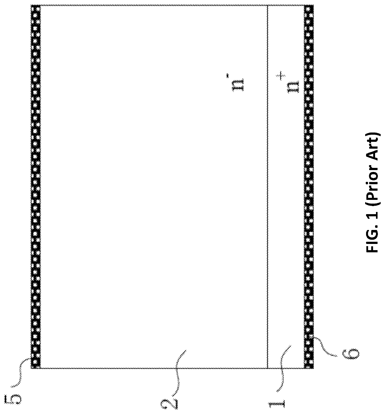
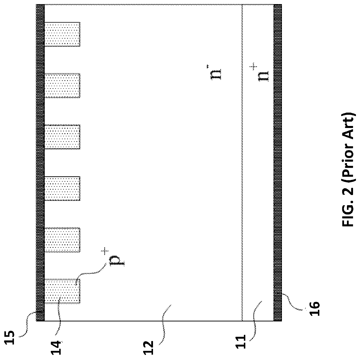
CROSS-REFERENCE TO RELATED APPLICATIONS[0001]This application claims priority under 35 U.S.C. § 119 (e) to U.S. Provisional Patent Application Ser. No. 62 / 699,649, filed on Jul. 17, 2018, the entire contents of which are hereby incorporated by reference.FIELD OF THE INVENTION[0002]The present invention relates to a Scthottky diode, and more particularly to a Scthottky diode with double P-type epitaxial layers and the manufacturing method thereof without implantation process.BACKGROUND OF THE INVENTION[0003]A conventional Schottky diode, referring to FIG. 1, may include an ohmic contact 6, a substrate 1, an epitaxial layer 2, and a Schottky contact metal 5. The Schottky contact metal 5 can be made of aluminum, titanium, nickel, silver or other metals. The substrate and epitaxial layers are usually doped with N-type impurity. A Schottky junction is formed between the Schottky contact metal 5 and epitaxial layer 2.[0004]The Silicon Carbide (SiC) Schottky diode is widely accepted in rec...

Claims


Application Information

Patent Timeline
IPC IPC(8): H01L29/16H01L29/66H01L29/872H01L29/45
CPCH01L29/1608H01L29/66143H01L29/872H01L29/45H01L29/0615H01L29/0619H01L29/6606
Inventor REN, NAZUO, ZHENGLI, RUIGANG
Owner AZ POWER INC
Why Eureka
Try Eureka