Dyed photoresists and methods and articles of manufacture comprising same

a technology of photoresists and dyes, applied in the field of new photoresist compositions, can solve the problems of unsatisfactory photoresist resolution, inability to provide such high-resolution fine line images, and often limiting the resolution of image patterned, so as to reduce the reflection of exposure radiation

Inactive Publication Date: 2006-12-12
SHIPLEY CO LLC
View PDF26 Cites 3 Cited by
  • Summary
  • Abstract
  • Description
  • Claims
  • Application Information

AI Technical Summary

Benefits of technology

[0012]The present invention provides new photoresist compositions that in general comprise a resin binder, a photoactive component, particularly an acid generator, and a dye material that contains one or more chromophores that can reduce undesired reflections of exposure radiation. Preferred dye compounds are polymeric materials (generally referred to herein as “resin dyes”) that include one or more chromophores that effectively absorb deep UV exposure radiation.
[0015]It has been found that use of a dye resin of the invention in a photoresist imparts significant lithographic improvements to the resist, including substantial reductions of undesired reflections of exposure radiation and enhanced resolution and masking linearity of developed resist images. See the results of the examples which follow.

Problems solved by technology

However, many current photoresists are not capable of providing such highly resolved fine line images.
For example, reflection of activating radiation used to expose a photoresist often poses limits on resolution of the image patterned in the photoresist layer.
Reflection of radiation from the substrate / photoresist interface can produce variations in the radiation intensity in the photoresist during exposure, resulting in non-uniform photoresist linewidth upon development.
Radiation also can scatter from the substrate / photoresist interface into regions of the photoresist where exposure is not intended, again resulting in linewidth variations.
The amount of scattering and reflection will typically vary from region to region, resulting in further linewidth non-uniformity.
Due to radiation reflection at the photoresist / substrate interface, however, constructive and destructive interference is particularly significant when monochromatic or quasi-monochromatic radiation is used for photoresist exposure.
In such cases the reflected light interferes with the incident light to form standing waves within the photoresist.
In the case of highly reflective substrate regions, the problem is exacerbated since large amplitude standing waves create thin layers of underexposed photoresist at the wave minima.
The underexposed layers can prevent complete photoresist development causing edge acuity problems in the photoresist profile.
If the photoresist thickness is non-uniform, the problem becomes more severe, resulting in variable linewidth control.
Variations in substrate topography also give rise to resolution-limiting reflection problems.
Any image on a substrate can cause impinging radiation to scatter or reflect in various uncontrolled directions, affecting the uniformity of photoresist development.
As substrate topography becomes more complex with efforts to design more complex circuits, the effects of reflected radiation become more critical For example, metal interconnects used on many microelectronic substrates are particularly problematic due to their topography and regions of high reflectivity.
Thus, the use of the shorter wavelengths has exacerbated the problems of reflection from a substrate surface.

Method used


Image

  • Dyed photoresists and methods and articles of manufacture comprising same
  • Dyed photoresists and methods and articles of manufacture comprising same
  • Dyed photoresists and methods and articles of manufacture comprising same

Examples


example 1

Preparation of Preferred Dye Resins

1. Preparation of Monomers with Chromophores.

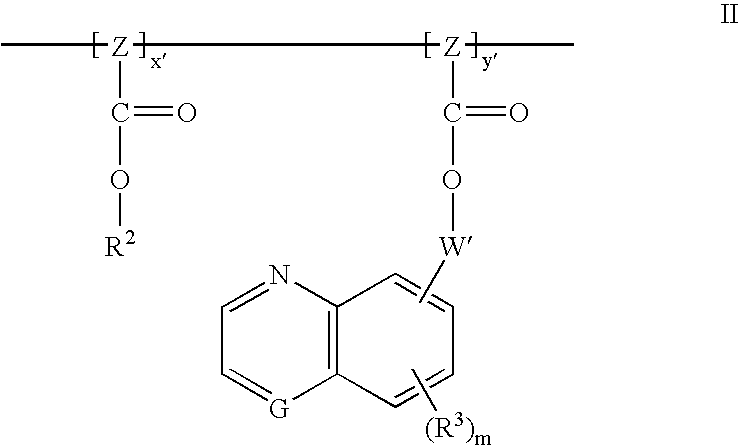
[0077]A. Preparation of Chloroxine Methacrylate.

[0078]A 500 ml round bottom flask equipped with magnetic stirrer and nitrogen inlet was charged with 5.0 g (0.0234 mol) 5.7 dichloro-8-hydroxyquinoline (chloroxine), 2.01 (0.0234 mol)methacrylic acid, 500 ml methylene chloride, 1.43 g (0.5 eq.), 4-dimethylamino-pyridine (DMAP) and 6.72 g 1-(3-dimethylamino propyl)-3-ethylcarbodimide (EDCI). The reaction mixture was stirred under a blanket of nitrogen for 12 hours at 25° C. The product was purified by column chromatography (methylene chloride) to give a pale yellow solid (yield 67%).

[0079]B. Preparation of Methylanthracene Methacrylate

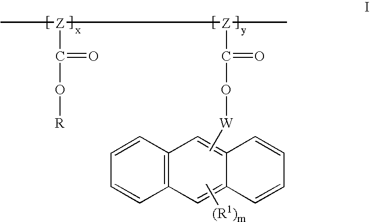
[0080]Methylanthracene methacrylate (CH3C(═CH2)CO2CH2-9-anthracene) was prepared as disclosed in Macromolecules, 17(2):235 (1984).

2. Preparation of Resins.

[0081]Methylanthracene methacrylate (ANTMA) / hydroxyethyl methacrylate (HEMA) copolymer (Formula III below) was prepared as ...

example 2

[0085]A solution consisting of 10.664 g of ANTMA / HEMA dye solution (5 wt % of ANTMA / HEMA resin of Formula III in ethyl lactate), 2.664 g polyhydroxystyrene-t-butylacrylate copolymer solids, 0.126 g Silwet™ L-7604 Surfactant solution (10% solids in Ethyl Lactate) and 6.525 g additional ethyl lactate was prepared. The solution was filtered through a 0.2 μm pore-size PTFE membrane filter.

[0086]Solutions of other dye materials were also formulated, using the same dye concentration as the ANTMA / HEMA copolymer. Those dyes are specified in Table I below. A sample with no dye material was also evaluated.

[0087]Quartz and silicon wafers were coated with the dyed polymer solutions for determining optical properties. Wafers were soft baked for 60 seconds at 100° C., vacuum hot plate, on a GCA MicroTrack coat and bake system. Silicon wafers were used for thickness and cauchy coefficient determinations. Absorbance spectra from 200 nm to 500 nm were taken on a Cary 13 UV-VIS Spectrophotometer; abs...

example 3

[0089]A photoresist composition (Resist 1) consisting of 6.083 g polyhydroxystyrene-t-butylacrylate copolymer solids, 2.432 g di-t-butylphenyliodonium camphorsulfonate photoacid generator solution (10 wt % solids in ethyl lactate), 0.136 g of a tetrabutyl ammonium hydroxide lactate solution (10 wt % solids in ethyl lactate), 0.181 g ANTMA / HEMA dye solution (34 wt % solids in 37.5 vol % Anisole:62.5 vol % propylene glycol monomethyl ether acetate), 0.322 g Silwet™ L-7604 Surfactant solution (10 wt % solids in ethyl lactate) and 30.850 g additional ethyl lactate was prepared.

[0090]Two additional photoresists (Resist 2 and Resist 3) were formulated in the samme manner as for Resist 1 and described about, except the amount of ANTMA / HEMA dye solution was varied to adjust the optical density of the photoresist film: Resist 2 contained 0.524 g of the ANTMA / HEMA dye solution and Resist 3 contained 0.864 g of the ANTMA / HEMA dye solution. Resists 1–3 thus contained 1, 3% and 5% dye solids (wt...


PUM

PropertyMeasurementUnit
weight average molecular weightaaaaaaaaaa
optical densityaaaaaaaaaa
mole fractionaaaaaaaaaa

Abstract

The present invention provides new photoresist compositions that comprise a resin binder, a photoactive component, particularly an acid generator, and a dye material that contains one or more chromophores that can reduce undesired reflections of exposure radiation. Preferred dye compounds are polymeric materials that include one or more chromophores such as anthracene and other polycyclic moieties that effectively absorb deep UV exposure radiation.

Description

BACKGROUND OF THE INVENTION[0001]1. Field of the Invention[0002]This invention relates to new photoresist compositions particularly suitable for deep U.V. exposure and having the capability of forming highly resolved features of submicron dimension.[0003]2. Background Art[0004]Photoresists are photosensitive films for transfer of images to a substrate. They form negative or positive images. After coating a photoresist on a substrate, the coating is exposed through a patterned photomask to a source of activating energy such as ultraviolet light to form a latent image in the photoresist coating. The photomask has areas opaque and transparent to activating radiation that define a desired image to be transferred to the underlying substrate. A relief image is provided by development of the latent image pattern in the resist coating. The use of photoresists is generally described, for example, by Deforest, Photoresist Materials and Processes, McGraw Hill Book Company, New York (1975), and...

Claims


Application Information

Patent Timeline
Patent Type & Authority Patents(United States)
IPC IPC(8): G03F7/04C08F20/10C08L33/06C09B69/10G03F7/004G03F7/038G03F7/039G03F7/09G03F7/30H01L21/027
CPCG03F7/0045G03F7/039G03F7/091Y10S430/106Y10S430/111Y10S430/127
Inventor MORI, JAMES MICHAELTHACKERAY, JAMES W.SINTA, ROGER F.BELL, ROSEMARYMILLER-FAHEY, ROBIN L.ADAMS, TIMOTHY G.ZYDOWSKY, THOMAS M.PAVELCHEK, EDWARD K.DOCANTO, MANUEL
Owner SHIPLEY CO LLC
Why Eureka
Try Eureka