Electrostatic capacitive touch pad

a capacitive touch pad, electrostatic technology, applied in the direction of static indicating devices, instruments, electrical apparatus construction details, etc., can solve the problems of impaired flexibility affecting etc., and achieve the effect of stabilizing the operation performance of the touch pad

Active Publication Date: 2006-12-19
ALPS ALPINE CO LTD
View PDF3 Cites 7 Cited by
  • Summary
  • Abstract
  • Description
  • Claims
  • Application Information

AI Technical Summary

Benefits of technology

[0023]By adopting such a constitution, it can prevent an effect to the wiring patterns formed on a surface of the first film substrate due to a static electricity generated in the vicinity of the touch pad arranged in the keyboard or the like, thereby stabilizing the operation performance of the touch pad.

Problems solved by technology

However, the conventional touch pad is likely to generate a connection failure, then causes the potential of the shield layer to be unstable, thereby adversely affecting the operation performance of the touch pad, since the shielding aluminum sheet was attached to the rear surface of the resultant touch pad and the aluminum sheet was connected to the ground electrode of the keyboard or the like, when it is arranged in the keyboard or the like of a PC.
In addition, there was a problem in that the aluminum sheet is attached to the rear surface of the touch pad and then the flexibility of the touch pad is impaired.

Method used


Image

  • Electrostatic capacitive touch pad
  • Electrostatic capacitive touch pad
  • Electrostatic capacitive touch pad

Examples


Embodiment Construction

[0030]Hereinafter, embodiments of a touch pad according to the present invention will be described in detail with reference to the accompanying drawings.

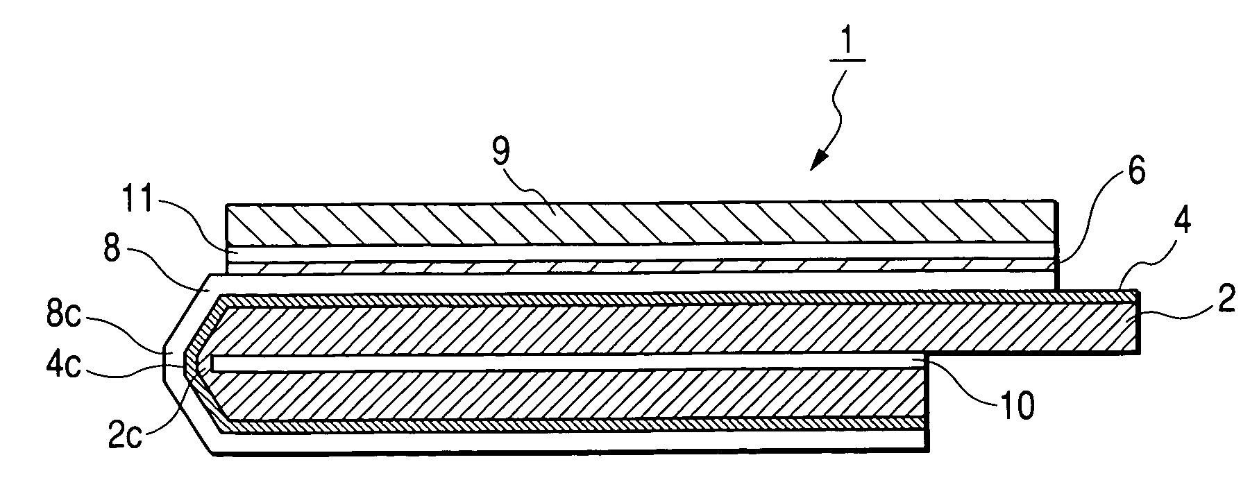
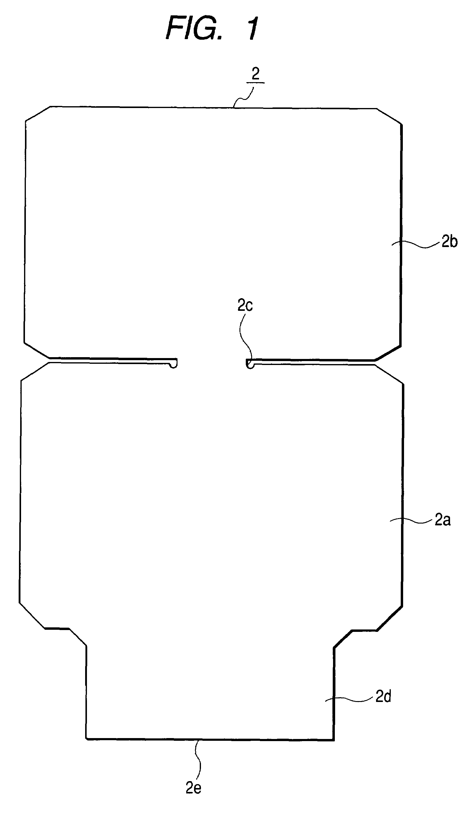
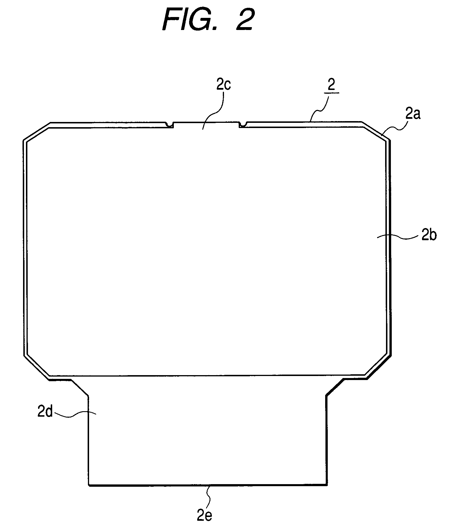
[0031]FIG. 1 is a plan view showing an embodiment of a film substrate of a touch pad according to the present invention. FIG. 2 is a rear view showing the bent film substrate of the embodiment. FIG. 3 is a circuit wiring view showing a Y electrode layer of one type of wiring pattern. FIG. 4 is a plan view showing an insulating film in the embodiment. FIG. 5 is a view showing only circuit wiring lines of an X electrode layer of the other wiring pattern. FIG. 6 is an exploded perspective view of the touch pad in the embodiment.

[0032]A shield layer of a touch pad 1 according to the present embodiment is formed by connecting each longitudinal side of an approximately quadrangular first film substrate 2a and an approximately quadrangular second film substrate 2b through a bent portion 2c to form a film substrate 2 made of an insulating s...


PUM


Abstract

On a surface of a film substrate made of an insulating synthetic resin, which is formed by connecting an approximately quadrangular first film substrate and an approximately quadrangular second film substrate through a bent portion, a ground electrode formed to cover at least a part of the second film substrate, and a first electrode layer formed of one of the wiring patterns on a part of the first film substrate are formed. An insulating film made of an insulating resin is formed on the first electrode layer, a second electrode layer formed of the other of the wiring patterns is formed on a surface corresponding to the part of the first film substrate of the insulating film, and the film substrate, the first electrode layer and the insulating film are bent in the bent portion such that the rear surfaces of the film substrate face each other.

Description

[0001]This application claims the benefit of priority to Japanese Patent Application No. 2003-178142, herein incorporated by reference.BACKGROUND OF THE INVENTION[0002]1. Field of the Invention[0003]The present invention relates to an electrostatic capacitive touch pad used, for example, as a pointing device of a personal computer, and more specifically, to a touch pad which is capable of ensuring flexibility, and stabilizing a connection with a ground electrode on a product and a potential of a shield layer.[0004]2. Description of the Related Art[0005]The conventional touch pad has a film substrate made of an insulating synthetic resin sheet such as PET (polyethyleneterephthalate) serving as a detection substrate. On one side of the film substrate, an extension portion protruding to one side is formed. On the film substrate, an X electrode layer and a Y electrode layer are formed as two types of wiring patterns, thereby detecting an electrostatic capacity.[0006]In more detail, an X...

Claims


Application Information

Patent Timeline
Patent Type & Authority Patents(United States)
IPC IPC(8): G09G5/00G06F3/044G06F3/03G06F3/033G06F3/041H05K7/06
CPCG06F3/03547G06F3/044G06F3/0445
Inventor SHIGETAKA, HIROSHI
Owner ALPS ALPINE CO LTD
Why Eureka
Try Eureka